
Paperis Articles
Semiconductors and the p-n Junction — An Empty Space in a Full Parking Garage, a Line Crossed Only One Way
A semiconductor is a material whose ability to conduct changes with heat, light and a few added atoms. Join an n-type piece with spare electrons to a p-type piece with empty spaces, and the boundary sends current only one way. The same principle underlies light-emitting devices and solar cells, though real devices use materials chosen for each job.
Your field's papers, as audio
Pick your fields and journals — Paperis summarizes the key papers and turns them into audio. Listen on your commute.
Start Paperis free →Semiconductors and the p-n Junction — An Empty Space in a Full Parking Garage, a Line Crossed Only One Way
Garden Lights
Some garden lights collect electricity by taking in sunlight during the day and use that electricity to turn on a light when the sun goes down. By day, they turn light into electricity; by night, they turn electricity into light. Two completely opposite tasks happen inside one single object.
Both tasks rely on the same type of structure. It is the boundary where two pieces with different electrical conduction properties are joined together. This article follows what that boundary is, why it sends electricity in only one direction, and how it gives off and receives light.
The two joined pieces are materials of the same family. A semiconductor is a material sitting somewhere between a metal, through which electricity flows well, and glass, through which it hardly flows at all, and depending on the conditions, it either lets electricity through or blocks it.
The Completely Full First Floor
First, let us look at a piece of pure silicon. When cooled to a very low temperature, pure silicon acts like an insulator and hardly conducts electricity at all (OpenStax University Physics Volume 3 9.5). To see why, we have to look inside the material. An atom is a particle made of a small nucleus and electrons around it. Electrons carry a negative (−) charge, and electricity flowing means that these charged particles are moving in one direction.
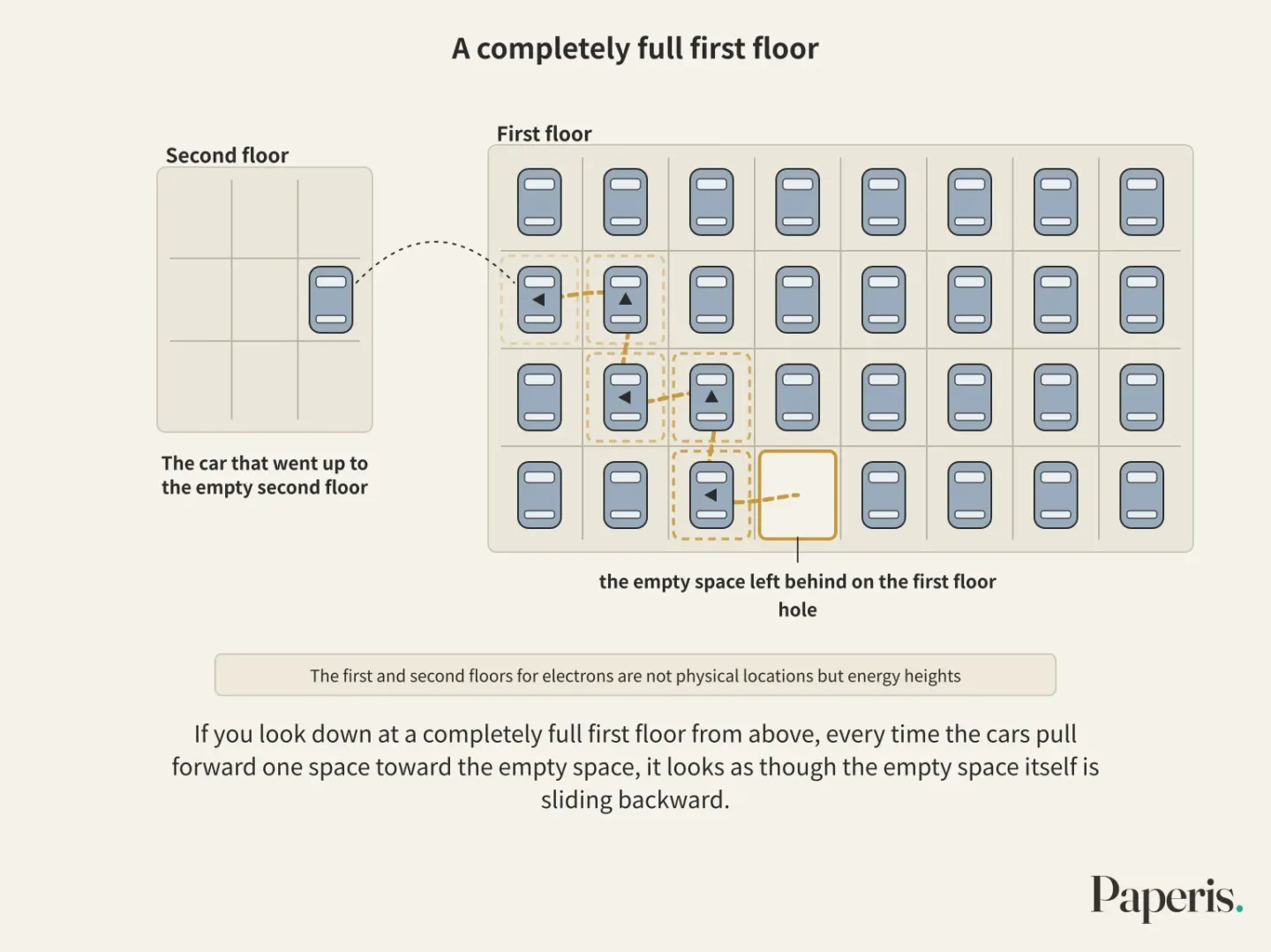
Let us picture the electrons inside silicon as cars parked in a two-story parking garage. The first floor, where the cars are parked, is packed tight with no empty spaces, while the second floor above it is completely empty. On a completely full first floor, no car has a space to move to, so no electricity flows (OpenStax University Physics Volume 3 9.5).
Then, how do we make it conduct? We just need to drive a single car up to the second floor. When we heat pure silicon, some of the electrons on the first floor absorb heat and jump up to the second floor, which is why the warmer it gets, the better it conducts electricity (DOI: 10.1103/physrev.75.865). Light does the exact same thing. In a semiconductor that has absorbed light, electrons break loose and move, and the empty spaces they leave behind make electricity flow even better (OpenStax Physics 21.2).
The moment a single car goes up, two things become able to move. The car that went up to the empty second floor, and the empty space left behind on the first floor. A hole is the empty space left behind when an electron departs. If you look down at a completely full first floor from above, every time the cars pull forward one space toward the empty space, it looks as though the empty space itself is sliding backward. Holes inside a semiconductor move by shifting places in this exact way, and they move as if they carry a positive (+) charge (OpenStax University Physics Volume 3 9.6).
There is a height that must be cleared for a car to reach the second floor. Between the first floor and the second floor, there is nowhere for a car to park. The band gap is an energy range within a material where electrons cannot stay at all. The height between the floors of the parking garage is the band gap. In a semiconductor, even at room temperature, some electrons use just heat alone to clear this height and reach the second floor (OpenStax University Physics Volume 3 9.5).
The name "semiconductor" easily sounds like it means electricity only half-flows. The usefulness of a semiconductor lies in the fact that its degree of conduction changes depending on conditions such as heat, light, and mixed-in atoms.
The Car the Guest Brought In, the Space Left Empty
Can we make it conduct on purpose without waiting for heat or light? In 1949 measurements looking into silicon mixed with a little boron or phosphorus using X-rays, the mixed atoms sat right in the places of the silicon atoms (DOI: 10.1103/physrev.75.865). Doping is the act of mixing a tiny amount of other atoms into silicon to change how well electricity flows.
The two guests used in this measurement worked in opposite directions. Phosphorus was the side that donated electrons, and boron left behind one empty space for each atom (DOI: 10.1103/physrev.75.865). In the parking garage picture, phosphorus is a guest driving in more cars, and boron is a guest leaving their own space on the first floor empty. For the guest's car and the empty space to start moving takes much less energy than crossing the band gap (DOI: 10.1103/physrev.75.865).
The mixed atoms make their own energy spots inside the band gap, right next to the first or second floor (OpenStax University Physics Volume 3 9.6). Measured in silicon mixed with just a little arsenic or boron, the energy it takes to go back and forth between those spots and the nearby floors was very small (DOI: 10.1103/physrev.96.28). Saying there is nowhere for electrons to stay in the band gap is something said about a pure crystal.
An n-type semiconductor is a semiconductor made by mixing in atoms with one more outer electron, so that the remaining electrons mainly carry electricity. A p-type semiconductor is a semiconductor made by mixing in atoms with one fewer outer electron, so that the resulting holes mainly carry electricity. The n and p in the names point to whether the electricity of the main carriers is negative or positive (OpenStax University Physics Volume 3 9.6). In this way, doping decides both the degree of conduction and whether electrons or holes are the main characters carrying electricity.
The amount mixed decides the number of particles. In a certain temperature range, the mixed atoms all give up their own share of electrons or empty spaces, so within that range, even if the temperature changes, the number of particles matches the net number of mixed atoms (DOI: 10.1103/physrev.75.865). When it gets hotter than that, electrons rising from the first floor by heat increase, and it starts conducting in the same way as pure silicon (DOI: 10.1103/physrev.75.865). However, when the temperature is low, the mixed atoms also block the path of the particles, so the particles moved better in purer samples (DOI: 10.1103/physrev.75.865). How to actually put the atoms to be mixed into the silicon continues in another part of this series, the part covering the process.
The Day Two Parking Garages Are Joined
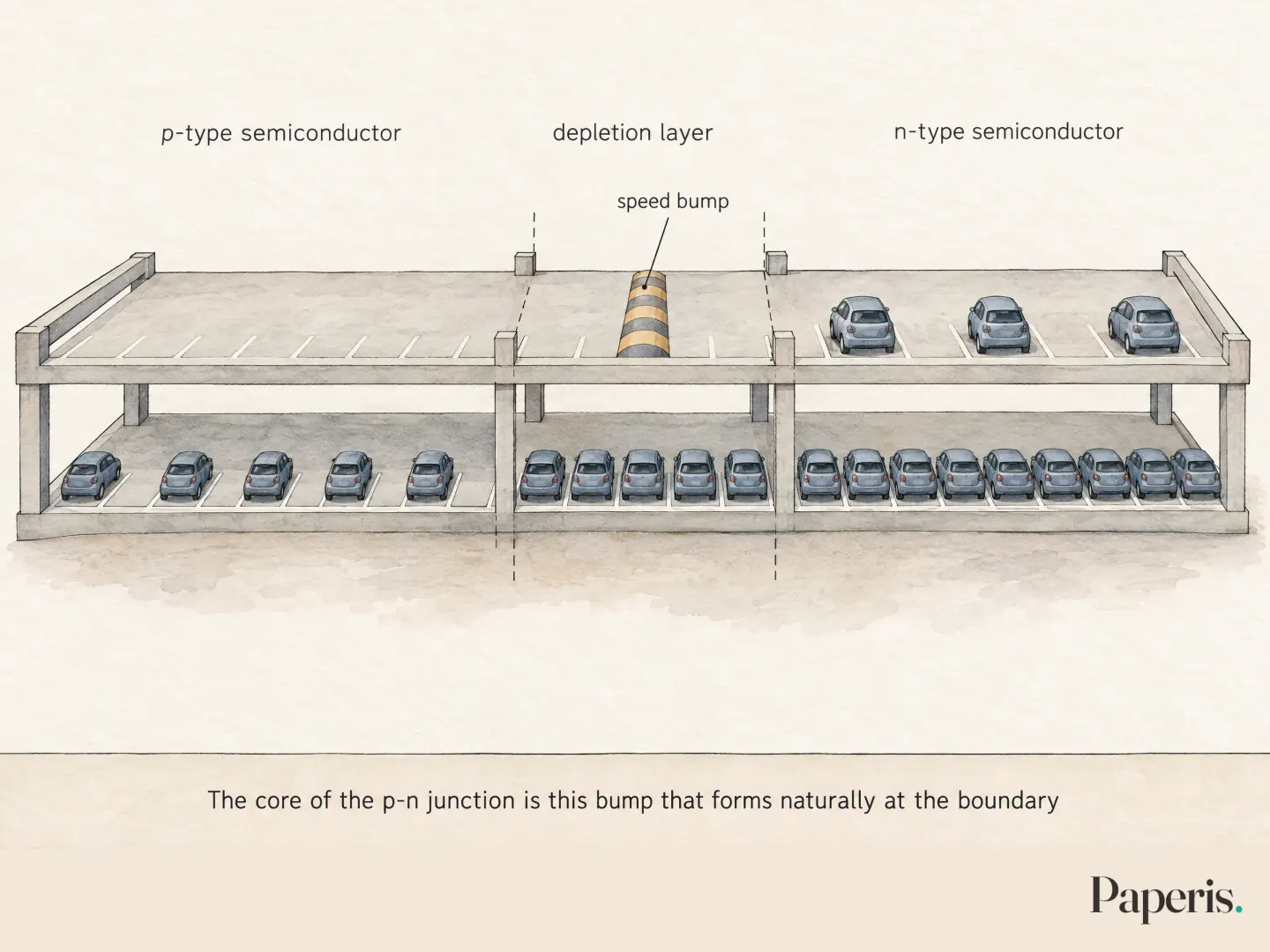
Now the n-type parking garage and the p-type parking garage are joined together without a wall. At the boundary, when a car from the n-side meets an empty space on the p-side and parks in it, both the moving car and the empty space disappear together (OpenStax University Physics Volume 3 9.7). A p-n junction is the boundary where a p-type semiconductor and an n-type semiconductor are put together.
The depletion layer is a thin band emptied out as the moving electrons and holes escape from both sides of the p-n junction. An electric field is set up across this band, and that electric field prevents cars from the n-side from crossing over any further (OpenStax University Physics Volume 3 9.7).
In terms of the parking garage, it is as if a speed bump has risen right at the boundary. This bump forms naturally as a result of cars crossing over to fill empty spaces. The core of the p-n junction is this bump that forms naturally at the boundary.
Which Way to Connect the Battery
This boundary, with its bump, becomes a useful device just as it is. A diode is a device made with a p-n junction that allows current to flow in only one direction. Why does it flow in only one direction? There are two ways to connect a battery across both ends of this boundary. The forward direction is connecting the positive terminal of the battery to the p-type side, and the reverse direction is connecting the positive terminal to the n-type side.
When connected in the forward direction, it is like the bump has been lowered so cars cross the boundary again and current flows easily, and when connected in the reverse direction, it is like the bump has risen higher so the cars crossing are almost entirely cut off (OpenStax University Physics Volume 3 9.7).
This boundary also connects to other devices. A transistor is a tiny switch turned on and off with electricity. A principle similar to the p-n junction forms the basis of the bipolar transistor, the first transistor to see major use (DOI: 10.1093/9780198921004.003.0009). When making silicon transistors, mixed atoms are also added to create p-n junctions and doped regions (DOI: 10.1109/5.658764). How transistors inside chips turn on and off today is covered in "A Transistor Is a Switch — A Tiny Faucet You Open and Close with Electricity".
Sink Down for Light, Lift Up for Electricity
While current flows in the forward direction, near the boundary, electrons crossing over from the n-side meet holes on the p-side. When an electron on the second floor sinks down into an empty space on the first floor, it gives off energy, and that energy can emerge as light. Light-emitting devices rely on electrons and holes meeting and combining to produce light in this way (DOI: 10.1021/acs.nanolett.5b00235). A light-emitting diode is a diode made so that electrons and holes meet at the junction to emit light, commonly called an LED.
What color comes out depends on the material. Making blue light required a semiconductor with a large band gap, and metal nitrides like gallium nitride were candidates. It was difficult to make good-quality crystals of this material, and there was no way to make it p-type. Overcoming these two obstacles, bright blue LEDs were already out on the market by around 1995 (DOI: 10.1126/science.267.5194.51). Without p-type there is no p-n junction, so doping was one reason why blue light was delayed.
One way to get white light is to coat yellow-emitting fluorescent material evenly over a blue LED chip and mix the two lights (DOI: 10.1149/1.1535207). Development continued for over 60 years from 1940, when the first semiconductor p-n junction was discovered, and a 2008 review evaluates that the most efficient white LED light sources greatly surpassed existing lighting technology (DOI: 10.1109/jlt.2008.923628).
This time we go in reverse. When sunlight is absorbed, an electron on the first floor climbs up to the second floor, creating an electron and a hole (DOI: 10.1109/jphotov.2012.2198434). A solar cell is a device that makes electricity by separating the electrons and holes created upon receiving light. There are two classes of solar cells, and conventional types like silicon solar cells do that job at the p-n junction (DOI: 10.1021/jp022507x).
In a silicon solar cell, electrons and holes are created throughout the semiconductor lump, and only after arriving at the junction do they separate from each other (DOI: 10.1021/jp022507x). The spot where they separate is the bump we saw earlier.
If you break the circuit, the electrons and holes have nowhere to go and pile up, and in an ideal case they meet again and emit as much light as the incoming sunlight (DOI: 10.1109/jphotov.2012.2198434). The more the piled-up electrons and holes disappear through other paths without emitting light, the more the accumulated amount decreases, and the voltage the solar cell can produce is also trimmed down (DOI: 10.1109/jphotov.2012.2198434). Therefore, a 2012 theoretical analysis concludes that for a solar cell to approach the theoretical limit of efficiency, it must also be an excellent light-emitting diode (DOI: 10.1109/jphotov.2012.2198434). Depending on how it is used, a p-n junction can become a device that emits light, or a device that receives light and produces electricity. However, actual devices choose separate materials depending on their use. The bright blue LED we saw earlier was made of gallium nitride (DOI: 10.1126/science.267.5194.51).
Once Again in Front of the Garden Light
We look at the garden light again after the sun has gone down. If that light is an LED, electricity is applied in the forward direction across the boundary of a small piece so that current flows, and electrons that have crossed over meet holes and settle down to emit light. If the daytime panel is a silicon solar cell, electrons and holes created by sunlight reach the boundary and split apart, and their flow gathers into electricity. Both tasks happen at the boundary where the side with surplus electrons and the side with remaining empty spaces touch.
The parking garage picture differs from reality in four places. First, the floors of a parking garage are upper and lower spaces, but the first and second floors for electrons are not physical locations but energy heights (OpenStax University Physics Volume 3 9.5). An electron that has climbed to the second floor does not move upward inside the crystal. Second, an empty parking space carries nothing, but a hole behaves as though it carries positive electricity. Still, a hole is merely a space vacated by an electron (OpenStax University Physics Volume 3 9.6).
Third, electrons are not individually distinguishable like cars with license plates, and there is no driver. Stopping in front of the boundary is also due to the electricity applied there (OpenStax University Physics Volume 3 9.7). Fourth, the bump at the boundary is not a wall. In the reverse direction, current simply barely flows; it is not cut off as if sliced with a knife (OpenStax University Physics Volume 3 9.7).
To summarize, a semiconductor is a material whose degree of conductivity changes according to conditions. When we create a side with surplus electrons and a side with empty spaces by mixing atoms and join them together, that boundary selects the direction of electricity. By adding materials suited to the application on top of this same principle, we make devices that emit light and solar cells that turn light into electricity.
Where to Look Next
Transistors, which are tiny switches turned on and off with electricity, are covered in "A Transistor Is a Switch — A Tiny Faucet You Open and Close with Electricity". If terms like current and voltage feel unfamiliar, you can start with "Voltage, Current, Power — What Goes All the Way Around Undiminished". Atoms and the electrons orbiting them lead into "Elements and Molecules — 118 Pieces of Type, Tens of Millions of Words".
The process of actually introducing atoms to be mixed into silicon is covered in "From Wafer to Chip — Stencils Laid Layer upon Layer, Squares Cut Out at the End", while why wide-bandgap materials are used to handle large amounts of electricity is covered in "Power Semiconductors — A Big Door That Never Stops Swinging, and the Heat of the Half-Open Moment".
Source Papers
- "University Physics Volume 3 — 9.5 Band Theory of Solids" (2016) — OpenStax University Physics Volume 3 9.5 — The energies of electrons in a solid bunch into bands with gaps between them; in a very cold semiconductor, the lower band is completely full and hardly conducts, while even at room temperature some electrons are thermally promoted to the upper band.
- "University Physics Volume 3 — 9.6 Semiconductors and Doping" (2016) — OpenStax University Physics Volume 3 9.6 — When an electron jumps to the upper band, it leaves behind an empty space (a hole) in the lower band that moves as if it carries a positive charge; impurity atoms create energy states near the bands within the band gap, and the type of semiconductor becomes n-type if negative carriers dominate or p-type if positive ones do.
- "University Physics Volume 3 — 9.7 Semiconductor Devices" (2016) — OpenStax University Physics Volume 3 9.7 — When n-type and p-type materials touch, electrons and holes meet and vanish at the boundary, creating a thin charged layer (the depletion region) that blocks further charges from crossing; applying an external voltage in one direction makes current flow easily while the opposite direction stops it almost entirely, turning it into a diode.
- "Physics — 21.2 Einstein and the Photoelectric Effect" (2020) — OpenStax Physics 21.2 — When a semiconductor absorbs light, electrons are knocked free and holes are left behind, increasing its conductivity.
- "Electrical Properties of Pure Silicon and Silicon Alloys Containing Boron and Phosphorus" (1949) — DOI: 10.1103/physrev.75.865 — X-rays confirm that boron and phosphorus substitute into silicon sites, where one boron atom equals one acceptor level, and the acceptor ionization energy is much smaller than the band gap; high-temperature conduction is due to thermally excited electrons, the saturation region just below the intrinsic range has carrier concentration equal to net impurity concentration (independent of temperature in that range), lower temperatures show higher mobility in purer samples due to impurity scattering, and resistance and Hall measurements separately determine electron and hole concentrations and mobilities.
- "Electrical Properties of Silicon Containing Arsenic and Boron" (1954) — DOI: 10.1103/physrev.96.28 — Ionization energies of arsenic donor and boron acceptor levels are small (at low impurity concentrations).
- "Principles of semiconductor devices" (2024) — DOI: 10.1093/9780198921004.003.0009 — Starting from the p-n junction (equilibrium, forward bias, and reverse bias), it shows that similar principles form the basis of the bipolar transistor, the first important transistor (textbook chapter).
- "History of some early developments in ion-implantation technology leading to silicon transistor manufacturing" (1998) — DOI: 10.1109/5.658764 — From the technology of creating silicon transistor p-n junctions and doped regions via ion implantation until it became mainstream in integrated circuit manufacturing.
- "Efficient Light-Emitting Diodes Based on Nanocrystalline Perovskite in a Dielectric Polymer Matrix" (2015) — DOI: 10.1021/acs.nanolett.5b00235 — Electroluminescence in light-emitting devices relies on the meeting of electrons and holes and the radiative recombination that emits light (introductory general principles).
- "High-Luminosity Blue and Blue-Green Gallium Nitride Light-Emitting Diodes" (1995) — DOI: 10.1126/science.267.5194.51 — Blue light requires a large band gap; the hurdles for the gallium nitride family were material quality and the lack of p-type doping, both of which were recently overcome so that bright blue LEDs are now commercially available.
- "Y3Al5O12:Ce0.05 Phosphor Coatings on Gallium Nitride for White Light Emitting Diodes" (2003) — DOI: 10.1149/1.1535207 — Mixing the blue light of a gallium nitride chip with the light of a yellow phosphor yields white light, which requires uniform coating and optimal thickness.
- "History, Development, and Applications of High-Brightness Visible Light-Emitting Diodes" (2008) — DOI: 10.1109/jlt.2008.923628 — Over 60 years of development from the discovery of the first semiconductor p-n junction in 1940, with white light sources at its peak vastly outperforming conventional lighting (review).
- "Strong Internal and External Luminescence as Solar Cells Approach the Shockley–Queisser Limit" (2012) — DOI: 10.1109/jphotov.2012.2198434 — Absorbed sunlight generates electrons and holes that accumulate in an open circuit and ideally emit light, while non-radiative recombination drains the accumulation and limits voltage; for an outstanding solar cell to approach the theoretical limit, it must be an outstanding LED (theoretical analysis).
- "Excitonic Solar Cells" (2003) — DOI: 10.1021/jp022507x — Solar cells fall into two categories: conventional types like silicon p-n junctions and excitonic types, where conventional pairs are generated throughout the bulk and separate after reaching the junction.
Sources (14)
- University Physics Volume 3 — 9.5 Band Theory of Solids
- University Physics Volume 3 — 9.6 Semiconductors and Doping
- University Physics Volume 3 — 9.7 Semiconductor Devices
- Physics — 21.2 Einstein and the Photoelectric Effect
- Electrical Properties of Pure Silicon and Silicon Alloys Containing Boron and PhosphorusDOI 10.1103/physrev.75.865
- Electrical Properties of Silicon Containing Arsenic and BoronDOI 10.1103/physrev.96.28
- Principles of semiconductor devicesDOI 10.1093/9780198921004.003.0009
- History of some early developments in ion-implantation technology leading to silicon transistor manufacturingDOI 10.1109/5.658764
- Efficient Light-Emitting Diodes Based on Nanocrystalline Perovskite in a Dielectric Polymer MatrixDOI 10.1021/acs.nanolett.5b00235
- High-Luminosity Blue and Blue-Green Gallium Nitride Light-Emitting DiodesDOI 10.1126/science.267.5194.51
- Y3Al5O12:Ce0.05 Phosphor Coatings on Gallium Nitride for White Light Emitting DiodesDOI 10.1149/1.1535207
- History, Development, and Applications of High-Brightness Visible Light-Emitting DiodesDOI 10.1109/jlt.2008.923628
- Strong Internal and External Luminescence as Solar Cells Approach the Shockley–Queisser LimitDOI 10.1109/jphotov.2012.2198434
- Excitonic Solar CellsDOI 10.1021/jp022507x