Paperis Articles
From Wafer to Chip — Stencils Laid Layer upon Layer, Squares Cut Out at the End
Chips are not assembled one at a time. Many are made at once on a single round silicon plate, by repeating layer after layer a sequence of laying down a film, transferring a pattern, and etching or implanting atoms, and a defect at any of those steps can cut into the share of chips that work.
Your field's papers, as audio
Pick your fields and journals — Paperis summarizes the key papers and turns them into audio. Listen on your commute.
Start Paperis free →From Wafer to Chip — Stencils Laid Layer upon Layer, Squares Cut Out at the End
Where a Fingernail-Sized Piece Is Born
If you take apart a mobile phone, you will find a few black, fingernail-sized pieces attached to a green board. Such a single piece can contain around a billion tiny parts (DOI: 10.1149/2.0071511jss). That is a number that would take about 30 years to reach even if you assembled them nonstop, one per second, like putting together a watch.
In reality, many identical chips are arranged like a checkerboard on top of a single round plate, and very thin layers are stacked and etched all at once across the entire plate for every layer. The only moment they are made separately for each chip is the very last step, when they are cut out by compartment.
This article follows the path of that single plate as it makes a round through the factory. As a guide, we bring along a stencil. If you hold a stencil cut in the shape of a pattern against a wall, spray paint, and then remove the stencil, the pattern remains only on the cut-out spots. If you apply a different stencil for each color and repeat this process, you get a picture with multiple overlapping colors. A chip factory is a place that places many identical pictures side by side on a single large sheet of paper and repeats this process very many times.
A Lump Grown from Melted Silicon
The starting point is silicon. Silicon is a representative semiconductor used to make chips. A semiconductor is a material that sits roughly halfway between a metal, which conducts electricity well, and glass, which hardly conducts it at all; depending on the conditions, it either lets electricity through or blocks it.
The silicon used in chips must have its atoms lined up in rows without disruption. An ingot is a lump of silicon grown by solidifying melted silicon. The ingots used for chips are made by growing crystals from melted silicon so that the entire atomic arrangement is connected in a single mass, namely a single crystal. Other methods of making ingots by pouring them into molds and letting them solidify come with the problem that crystal defects and impurities develop while they grow (DOI: 10.1002/pip.2344). Slicing this lump thinly produces a wafer. A wafer is a thin, round silicon plate used to make chips. Sticking to the stencil analogy, the wafer is that large sheet of paper.
If the paper already has a flaw, no matter how well you print on it, it is useless. A defect is a flaw that can form on a wafer and prevent a chip from operating properly, encompassing fallen particles, residual chemicals, scratches, and disruptions within the crystal. Defects can arise starting from the stage of making the plate. Inside the melted silicon, fierce currents swirl, and in one experiment, applying a magnetic field to calm these currents made it possible to evenly adjust the amount of oxygen mixing into the crystal. Crystals low in oxygen developed fewer defects when later exposed to heat, and compared with plates grown through other methods, the performance and usable yield of several components made from those plates were also better (DOI: 10.1149/1.2113933, a 1985 experiment). Chip defects can begin right inside the material, even before entering the factory's first process.
The Room That Rules the Dust
The films applied onto a wafer are far thinner than the width of the patterns being etched. Therefore, defects as small as 1/100th of the pattern width must be controlled (DOI: 10.17764/jiet.1.31.2.9863780552351680, 1988 analysis). Even invisible particles become flaws on a chip.
A cleanroom is a workspace that filters out dust particles and chemical substances from the air, keeping them bounded below a set level. The targets being filtered include gas molecules as well. Sizes are measured in nanometers. A nanometer is 1 billionth of a meter. Based on a process generation around 2007, ammonia in the air had to be below 2.5 parts per billion, and the particle size to worry about went down to 23 nanometers (DOI: 10.4209/aaqr.2007.05.0030). Because airborne organic molecules also settle on the wafer surface, the factory measures them and filters them out using chemical filters (DOI: 10.1149/1.2147286).
Sometimes the source of contamination is the process inside the factory itself. Cases have been reported where corrosive gas leaked from a freshly carved wafer and soiled the surroundings (DOI: 10.4209/aaqr.2007.05.0030). A cleanroom is merely the foundation for lowering defects coming from the air, and paths for defects to enter remain open in the equipment, the chemicals, and every single process.
Deposition — Coating the Entire Plate with a Film
Now it is time to paint the background on the paper. Deposition is the process of evenly coating the wafer surface with a thin film of another substance. There are various methods, such as reacting gaseous raw materials on the surface to build them up, blowing vaporized substances to stick them on, and spinning and spreading a liquid, and the quality of the film largely depends on the substrate, temperature, and choice of raw materials (DOI: 10.1016/j.jmrt.2022.10.064). In modern device manufacturing, films are needed that can be controlled down to the thickness of just a few atomic layers and that evenly cover even the insides of valleys on bumpy surfaces (DOI: 10.1116/1.1622676).
There is also a way to grow a film instead of placing it on top. Thermal oxidation is the process of reacting a silicon wafer with oxygen at high temperatures to grow the surface silicon itself into a silicon oxide film. While deposition is bringing in a new substance from the outside and placing it on top, thermal oxidation is the underlying silicon itself becoming the film. Thermal oxidation is an important process in semiconductor manufacturing. In an experiment where a wafer intentionally contaminated with lithium was thermally oxidized, the lithium clearly affected the quality of the oxide film, showing that it can be harmful to devices (DOI: 10.1002/adem.202400396). Even in a single background coating, there are ways for defects to creep in.
Drawing and Carving — Carving Away the Spots Under the Stencil's Holes
Once a layer has been coated across the entire plate, it is necessary to decide which parts to keep and which parts to remove. Determining that boundary is lithography. Lithography is the process of transferring a circuit pattern onto silicon by shining light on it. First, a layer that reacts to light is spread on top of the film. A photoresist is a thin film whose properties change when it receives light. After shining the pattern and washing one side away, holes are punched in the photoresist in the shape of the pattern, which serves as the stencil. How light draws those fine lines is covered in "Lithography — Painting Circuits with a Brush of Light".
Once the stencil is in place, the layer underneath is scraped away. Etching is the process of using the remaining photoresist as a shield to carve away the underlying layer that it does not cover. Plasma is used for carving. Plasma is a state created by putting electrical energy into a gas, splitting it into particles that react extremely well. Chemically active particles in the plasma react with the film to carve it away, and this method is cleaner and more precise in its dimensions than the method of dissolving by dipping in a chemical solution (DOI: 10.1116/1.569137, 1977 review).
The carving work does not always end cleanly, either. Only the film meant to be carved must be carved while the underlying layer is preserved, it is necessary to figure out when to stop, and the carving speed varies depending on the area exposed at once. Residue may remain on the carved surface, or the atomic arrangement may be damaged by collisions with electrically charged particles (DOI: 10.1002/ppap.200400035). Patterns are determined by the actions of transferring and carving the image, and with each of those actions, room for flaws to occur arises as well.
Insertion — Shooting Atoms Through the Stencil's Holes
Instead of etching away, there are times when we insert. To make silicon do different jobs at different spots, we must mix in other atoms. Doping is the act of mixing tiny amounts of other atoms into silicon to change how well electricity flows through it. Which combinations change things in what ways is covered in another part of this series that deals with the p-n junction; here, we look at how they are inserted.
Ion implantation is a method where the atoms to be inserted are turned into charged particles, shot at high speed, and embedded beneath the wafer's surface. They do not get embedded where the stencil covers, but only go into the spots where holes are open. In terms of a cut-out stencil, it is the action of spraying paint through the holes so that it sinks deep into the paper.
The shot-in atoms can disrupt the crystal. In an experiment where antimony atoms were shot into silicon at room temperature, the path around every single atom was heavily damaged, and once the inserted amount crossed a certain line, the damaged spots overlapped so much that the atomic arrangement of that layer was completely scrambled. This layer's arrangement was readjusted only after being heated to a high temperature, and the inserted atoms properly settled into the silicon atoms' places. In the same experiment, when the wafer was implanted while heated, the disorder was very small (DOI: 10.1139/p67-339, 1967 experiment). Heat treatment is the step of heating the wafer to a high temperature to readjust the scrambled atomic arrangement and make the inserted atoms sit in their proper places.
Heat treatment has side effects as well. Silicon atoms that lost their places and squeezed in during implantation remain, and these atoms temporarily cause inserted atoms like boron or phosphorus to diffuse faster than usual during heat treatment. This phenomenon becomes a stumbling block when creating spots where the inserted atoms must be kept shallow and close to the surface (DOI: 10.1063/1.364452). The insertion action is a pair of shooting and repairing, and even while repairing, one must manage how far the inserted atoms spread.
Grind Flat, and Then Back to the Beginning
A surface that has repeatedly gone through stacking and carving develops variations in height. To properly place the stencil for the next layer, the base must be made even. Chemical mechanical polishing is a planarization process that flows chemical slurry over the wafer surface while rubbing it with a pad, mechanically scraping away the layer softened by the chemicals. For decades, it has been the most widely used planarization method in chip processing (DOI: 10.1007/s40544-013-0035-x). Even when creating the shallow trenches that electrically separate the roughly one billion components inside a single chip from one another, the oxide filling the trenches must be rapidly ground down until it stops precisely at the layer underneath (DOI: 10.1149/2.0071511jss). Grinding creates defects, too. Layers can peel, scratch, pit, or corrode, and these issues can cut down both the proportion of usable chips and their durability (DOI: 10.1007/s40544-013-0026-y).
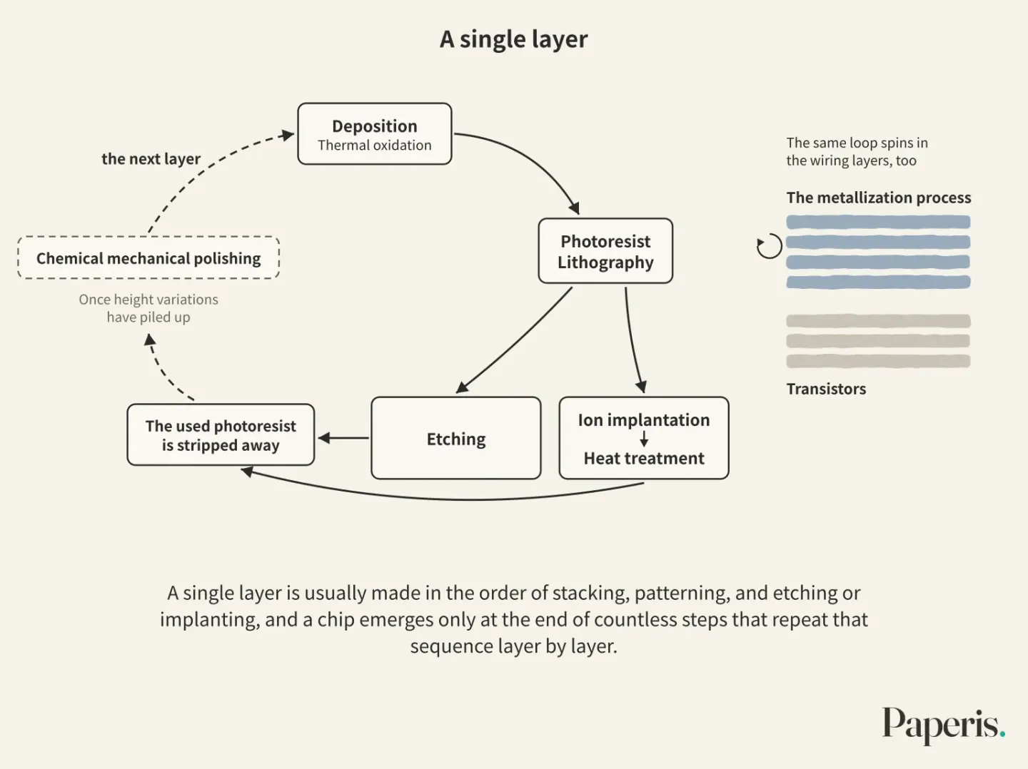
Now we follow a single point on the wafer as it makes a full loop. We deposit a film, apply photoresist, shine light to form a pattern, and etch away the opened areas or shoot atoms into them. The used photoresist is stripped away (DOI: 10.1116/1.569137). Once height variations have piled up, the surface is ground smooth, and the next layer begins as a new film is deposited.
In the very bottom layers, transistors are built. A transistor is a tiny switch turned on and off with electricity. Above them, metal lines connecting the transistors climb up layer by layer. The metallization process is the step where metal wiring layers are built on top after the transistors are finished. The same loop spins in the wiring layers, too. In the wiring layers, holes and trenches where the copper wiring will go are precisely etched into the insulating film (DOI: 10.1143/jjap.47.1435).
If you count these actions one by one as steps, there are very many of them. A typical fine process in 1988 already went through 250 steps (DOI: 10.17764/jiet.1.31.2.9863780552351680), and wafer manufacturing has grown even more complex since then (DOI: 10.1080/24725854.2017.1386337). A single layer is usually made in the order of stacking, patterning, and etching or implanting, and a chip emerges only at the end of countless steps that repeat that sequence layer by layer.
Getting Through All Those Steps Safely — Defects and Yield
The number a factory cares about most is yield. Yield is the proportion of manufactured chips that come out in a usable state. Not every defect kills a chip. A fatal defect is one that, by itself, makes a single chip unusable.
For a single chip to survive, it must pass safely through every single one of those steps without missing a single one. The more steps there are, the more the small losses piling up at each step add together. The more steps there are, the smaller the defects added by any single step must be. How small must they be? A 1988 analysis calculated that to achieve a 78% yield in a fine-pattern process passing through 250 steps, the fatal defects added by a single step must not exceed an average of 0.001 per square centimeter of the wafer. Only then, after passing through all 250 steps, will the remaining fatal defects stay under 0.25 per square centimeter (DOI: 10.17764/jiet.1.31.2.9863780552351680).
Just how tight is this single-step allowance? In the same analysis, merely leaving a wafer for an hour in a very clean grade (Class 1) cleanroom resulted in defects settling from the air that reached this single-step allowance. Steps where automated equipment handled the wafer or where it came into contact with chemicals and gases added far more defects than that (DOI: 10.17764/jiet.1.31.2.9863780552351680).
Yield is one of the core performance metrics companies use when managing their processes (DOI: 10.1080/00207540600596874). However, yield varies depending on how many steps there are and how small the patterns are (DOI: 10.17764/jiet.1.31.2.9863780552351680), and it is also influenced by how and where defects cluster across the wafer (DOI: 10.1080/00207540600596874). Yield is a core yardstick, but it is a number that can only be understood when you also know the conditions—such as what kind of chip was made and through what process.
A wafer with zero defects is the goal manufacturers aim for (DOI: 10.1109/tsm.2018.2825482). Because actual wafers contain a mix of random defects scattered without a clear cause, analyzing defects begins with separating these random defects from patterns that have an assignable cause (DOI: 10.1080/24725854.2017.1386337). As the 1988 calculation shows, defects must be kept constrained below the allowance each step is permitted to add (DOI: 10.17764/jiet.1.31.2.9863780552351680).
Measuring Along the Way, Drawing a Map
Equipment drifts little by little. Factories measure test wafers at set times to check equipment status, but with this method, they may fail to catch equipment quietly drifting between two measurements in time, and defects can form on the wafers made in the meantime. Therefore, a method was proposed to estimate the film thickness for each wafer in advance using the logs left by the equipment, and a study tested this method in a film deposition process (DOI: 10.1109/tmech.2007.897275).
Completed wafers undergo testing at each chip location to separate the good ones from the bad ones. A wafer map is a map that marks test results as good and bad for each chip location on a wafer. The results of neighboring chips tend to resemble each other, so patterns appear on the map, and patterns like scratch marks or ring shapes are signs that there is a traceable cause somewhere. As processes have become more complex, it has also become more common than before for different patterns to overlap on a single wafer (DOI: 10.1080/24725854.2017.1386337). The patterns formed by defects serve as clues for finding equipment issues or process instability (DOI: 10.1109/66.857947).
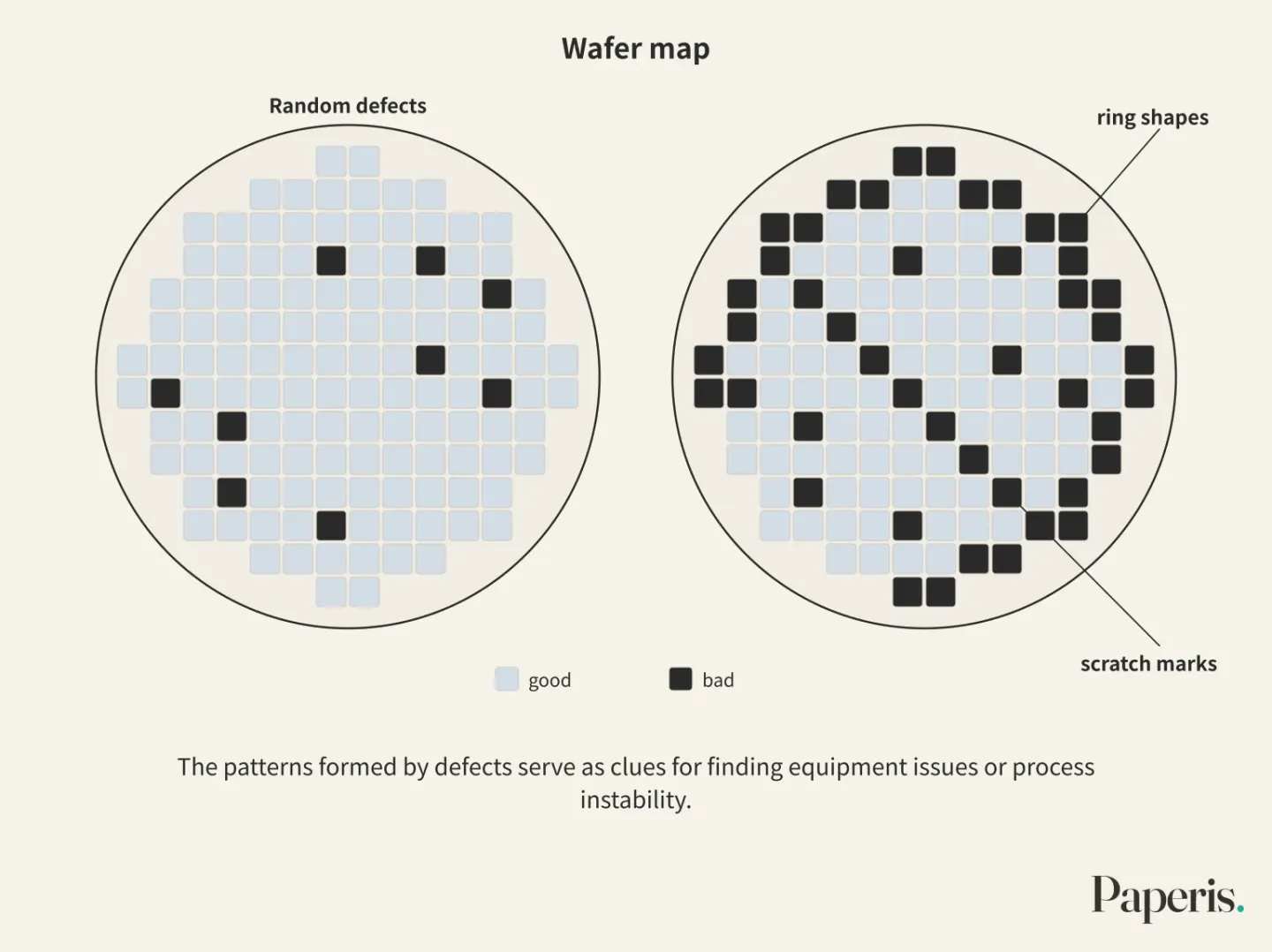
One of the tasks in raising yield is reading this map and tracing back to the step and equipment pointed to by the pattern.
Cutting Out Cell by Cell
The last step is cutting out. A die is a single piece of chip cut out from a wafer. The tested wafer is cut along the cell boundaries to separate it into dies, and only the dies confirmed to be functioning normally move on to the next stage. Wrapping the die and connecting it to the outside is picked up by another part of this series that covers packaging.
We have followed this path using the stencil analogy, but chip factories differ from stamping stencils. In wall painting, paint is added through the holes in a stencil, but in etching, the film where the stencil has holes is stripped away. A stencil held against a wall can be reused over and over once cut, but the photoresist stencil on the wafer is freshly created with light for each layer and stripped off after use. Paint simply sits on paper, but a chip's layers must be connected vertically by holes and metal to form a single circuit. And while a painting is still a painting even if it is a little blurry, a single flaw at just one of those many steps can render a chip unusable.
Many chips are made all at once on a single wafer, and the more steps there are, the more managing defects and taking measurements along the way determine the yield.
Where to Look Next
The patterning step of making the stencil continues in "Lithography — Painting Circuits with a Brush of Light". What the size of the patterns on the wafer and the name of a process generation are actually measuring is covered by "What Is "3 Nanometers" the Length Of? — Measuring a Chip's Name with a Tape Measure", and how the transistors built on the bottom layer turn on and off is covered by "A Transistor Is a Switch — A Tiny Faucet You Open and Close with Electricity". The process of grinding down the backside of a finished wafer can be found in "Turn the Power Around and the Heat Gets Trapped — The Bill for Grinding Away the Silicon Under the Transistors", and the process of directly bonding two surfaces together in "Nothing In Between — How Bonding Two Surfaces Directly Became the Center of the Process". What changes through doping is continued in "Semiconductors and the p-n Junction — An Empty Space in a Full Parking Garage, a Line Crossed Only One Way", and how the cut-out dies become a product is continued in "Packaging — A Chip Laid Face Down, a Three-Legged Race with Mismatched Strides".
Source Papers
- "Shallow Trench Isolation Chemical Mechanical Planarization: A Review" (2015) — DOI: 10.1149/2.0071511jss — Electrically isolating roughly 1 billion devices inside a chip with shallow trenches requires polishing that rapidly grinds down the oxide film and stops at the nitride film. Reducing defects after polishing remains a challenge.
- "About the origin of low wafer performance and crystal defect generation on seed-cast growth of industrial mono-like silicon ingots" (2012) — DOI: 10.1002/pip.2344 — Czochralski silicon wafers (for solar cells) are single crystals, whereas casting-grown ingots develop extension defects and impurities.
- "Czochralski Silicon Crystals Grown in a Transverse Magnetic Field" (1985) — DOI: 10.1149/1.2113933 — Suppressing turbulence in molten silicon with a magnetic field allows precise and uniform oxygen concentration, and low-oxygen crystals suffer fewer thermally induced defects while matching device characteristics and yields better than float-zone wafers.
- "The Effects of Contamination on Semiconductor Manufacturing Yield" (1988) — DOI: 10.17764/jiet.1.31.2.9863780552351680 — Defects must be controlled down to 1/100 of pattern width, and achieving a 78% yield (0.25 defects/cm²) across a 250-step process requires 0.001 defects/cm² or less per step. Equipment, chemicals, and gases add more defects than cleanroom air, and shrinking patterns requires lowering particle levels by about 10 times.
- "Case Study of Micro-Contamination Control" (2007) — DOI: 10.4209/aaqr.2007.05.0030 — Four contamination cases based on the 45nm generation, including ammonia under 2.5ppb, particles of interest at 23nm, and corrosive gases leaking from wafers immediately after dry etching.
- "Organic Airborne Molecular Contamination in Semiconductor Fabrication Clean Rooms" (2006) — DOI: 10.1149/1.2147286 — A review of surface deposition and measurement of organic airborne molecular contamination, alongside control strategies including chemical filters.
- "Atomic layer deposition and other thin film deposition techniques: from principles to film properties" (2022) — DOI: 10.1016/j.jmrt.2022.10.064 — A comparison of thin-film deposition methods such as physical and chemical vapor deposition, sputtering, and spin coating. Film quality depends heavily on the choice of substrate, temperature, and raw materials.
- "Atomic layer deposition of metal and nitride thin films: Current research efforts and applications for semiconductor device processing" (2003) — DOI: 10.1116/1.1622676 — Interest in atomic layer deposition has grown as modern device manufacturing demands nano-thin films that cover surfaces evenly at the atomic scale.
- "Influences and Diffusion Effects of Lithium Contamination during the Thermal Oxidation Process of Silicon" (2024) — DOI: 10.1002/adem.202400396 — Silicon thermal oxidation is a crucial process, and when intentionally lithium-contaminated wafers undergo thermal oxidation, lithium distinctly affects the quality of the oxide film and can harm devices.
- "Plasma etching in integrated circuit manufacture—A review" (1977) — DOI: 10.1116/1.569137 — Plasma etching, which carves with chemically active radicals in a glow discharge, is dry, clean, and offers better dimensional tolerances than wet etching. Plasma etching and photoresist stripping are compatible with the process. Fundamental understanding and equipment require further development.
- "Dry Etching of Electronic Oxides, Polymers, and Semiconductors" (2004) — DOI: 10.1002/ppap.200400035 — Reproducibility issues such as the loading effect, endpoint detection, and selectivity, alongside surface disturbances like polymer deposition, residues, and ion-induced displacement damage.
- "ION IMPLANTATION OF SILICON: I. ATOM LOCATION AND LATTICE DISORDER BY MEANS OF 1.0-MeV HELIUM ION SCATTERING" (1967) — DOI: 10.1139/p67-339 — Antimony implanted at room temperature creates damaged regions along its trajectory and becomes an amorphous layer at high doses, while heat treatment restores the lattice and seats it in substitutional sites.
- "Physical mechanisms of transient enhanced dopant diffusion in ion-implanted silicon" (1997) — DOI: 10.1063/1.364452 — Excess interstitial atoms generated by implantation cause transient enhanced diffusion of boron and phosphorus during heat treatment, and suppressing this helps form shallow junctions.
- "Chemical mechanical polishing: Theory and experiment" (2013) — DOI: 10.1007/s40544-013-0035-x — Chemical mechanical polishing has been the most widely used planarization method in integrated circuit manufacturing for decades, and its mechanism is complex.
- "Scratch formation and its mechanism in chemical mechanical planarization (CMP)" (2013) — DOI: 10.1007/s40544-013-0026-y — Film delamination, scratches, dishing, erosion, and corrosion during polishing become defects that degrade yield and reliability.
- "Developments of Plasma Etching Technology for Fabricating Semiconductor Devices" (2008) — DOI: 10.1143/jjap.47.1435 — A review of the transition from wet to dry etching and plasma etching applications including via holes and trenches for copper/low-k interconnect wiring processes.
- "A review of yield modelling techniques for semiconductor manufacturing" (2006) — DOI: 10.1080/00207540600596874 — Semiconductor manufacturing is a complex multi-step process, and yield models address spatial defects and radial yield loss while requiring a system-wide view.
- "Deep-Structured Machine Learning Model for the Recognition of Mixed-Defect Patterns in Semiconductor Fabrication Processes" (2018) — DOI: 10.1109/tsm.2018.2825482 — Manufacturers aim for defect-free wafers and trace causes through the spatial patterns of defects (proposing a mixed-pattern classification model).
- "Detection and clustering of mixed-type defect patterns in wafer bin maps" (2017) — DOI: 10.1080/24725854.2017.1386337 — Wafer bin maps mark test results as good/bad for each chip, and neighboring chips correlate spatially to form patterned causes (scratches, rings). Separating random defects is a challenge, and mixed patterns are more frequent than before.
- "A Novel Virtual Metrology Scheme for Predicting CVD Thickness in Semiconductor Manufacturing" (2007) — DOI: 10.1109/tmech.2007.897275 — Because equipment drift between scheduled measurements can be missed, we propose virtual metrology—predicting film thickness per wafer using equipment variables—and test it in chemical vapor deposition.
- "A neural-network approach to recognize defect spatial pattern in semiconductor fabrication" (2000) — DOI: 10.1109/66.857947 — Wafer defects are a primary cause of yield loss, and the spatial patterns of defects are clues to equipment problems or process variations.
Sources (21)
- Shallow Trench Isolation Chemical Mechanical Planarization: A ReviewDOI 10.1149/2.0071511jss
- About the origin of low wafer performance and crystal defect generation on seed-cast growth of industrial mono-like silicon ingotsDOI 10.1002/pip.2344
- Czochralski Silicon Crystals Grown in a Transverse Magnetic FieldDOI 10.1149/1.2113933
- The Effects of Contamination on Semiconductor Manufacturing YieldDOI 10.17764/jiet.1.31.2.9863780552351680
- Case Study of Micro-Contamination ControlDOI 10.4209/aaqr.2007.05.0030
- Organic Airborne Molecular Contamination in Semiconductor Fabrication Clean RoomsDOI 10.1149/1.2147286
- Atomic layer deposition and other thin film deposition techniques: from principles to film propertiesDOI 10.1016/j.jmrt.2022.10.064
- Atomic layer deposition of metal and nitride thin films: Current research efforts and applications for semiconductor device processingDOI 10.1116/1.1622676
- Influences and Diffusion Effects of Lithium Contamination during the Thermal Oxidation Process of SiliconDOI 10.1002/adem.202400396
- Plasma etching in integrated circuit manufacture—A reviewDOI 10.1116/1.569137
- Dry Etching of Electronic Oxides, Polymers, and SemiconductorsDOI 10.1002/ppap.200400035
- ION IMPLANTATION OF SILICON: I. ATOM LOCATION AND LATTICE DISORDER BY MEANS OF 1.0-MeV HELIUM ION SCATTERINGDOI 10.1139/p67-339
- Physical mechanisms of transient enhanced dopant diffusion in ion-implanted siliconDOI 10.1063/1.364452
- Chemical mechanical polishing: Theory and experimentDOI 10.1007/s40544-013-0035-x
- Scratch formation and its mechanism in chemical mechanical planarization (CMP)DOI 10.1007/s40544-013-0026-y
- Developments of Plasma Etching Technology for Fabricating Semiconductor DevicesDOI 10.1143/jjap.47.1435
- A review of yield modelling techniques for semiconductor manufacturingDOI 10.1080/00207540600596874
- Deep-Structured Machine Learning Model for the Recognition of Mixed-Defect Patterns in Semiconductor Fabrication ProcessesDOI 10.1109/tsm.2018.2825482
- Detection and clustering of mixed-type defect patterns in wafer bin mapsDOI 10.1080/24725854.2017.1386337
- A Novel Virtual Metrology Scheme for Predicting CVD Thickness in Semiconductor ManufacturingDOI 10.1109/tmech.2007.897275
- A neural-network approach to recognize defect spatial pattern in semiconductor fabricationDOI 10.1109/66.857947