
Paperis Articles
Power Semiconductors — A Big Door That Never Stops Swinging, and the Heat of the Half-Open Moment
Inside chargers and electric cars, what reshapes electricity is a big switch that turns on and off very often. The switch loses energy as heat both while it is on and at each moment it switches, and wide-bandgap silicon carbide and gallium nitride cut those losses while bringing their own problems of defects, cost and reliability.
Your field's papers, as audio
Pick your fields and journals — Paperis summarizes the key papers and turns them into audio. Listen on your commute.
Start Paperis free →Power Semiconductors — A Big Door That Never Stops Swinging, and the Heat of the Half-Open Moment
Why Chargers Get Warm
When you charge your phone overnight and unplug the charger in the morning, there are times when a lukewarm warmth remains in your hand. The charger converts the electricity coming from the wall outlet into electricity that the phone battery can receive. During that conversion, some of the electricity leaks out and warms the charger.
Electric vehicles do the exact same thing on a much larger scale. The electricity coming from the charger changes its shape once before being stored in the battery, and when driving, the electricity coming out of the battery changes its shape again to go to the motor that turns the wheels. The electricity generated by the rooftop solar panels also changes its shape before heading to the indoor wall outlet. In this way, electricity often changes its shape more than once before it is used.
At the very center of the device in charge of that work lies a switch. Its job is the same as the light switch in your room, but it moves by electrical signals instead of a human hand and turns on and off very frequently without resting. This article pictures that switch as a large door. When the door is closed, it must block the surging electricity, and when the door is thrown wide open, it must let a lot of electricity out all at once. And this door opens and closes without a break.
Changing the Shape of Electricity
We follow along starting from the scene of plugging an electric vehicle into a charger. First, we need three words that describe electricity. Voltage is the difference between two points that makes electricity flow, measured in volts. Spoken of in terms of a door, it is the push against a closed door.
Current is the flow of electricity along a wire, measured in amperes by how much passes a point in one second. Spoken of in terms of a door, it is the flow passing through the door. Power is the amount of energy electricity moves in one second, measured in watts.
The electricity coming out of a wall outlet and the electricity stored in a battery differ even in how they flow. Alternating current is electricity in which the direction of flow reverses back and forth many times even in a single second. Direct current is electricity that flows in only one direction. For example, one design that built an electric vehicle charger takes in 240-volt alternating current and outputs 200 to 450-volt direct current to the battery (DOI: 10.1049/iet-pel.2017.0467). Both the way it flows and the voltage change.
Power conversion is the work of turning alternating current and direct current into each other or raising and lowering voltage. When charging, alternating current turns into direct current, and when driving, the reverse conversion happens. An inverter is a device that changes direct current into alternating current. In an electric vehicle, an inverter sits between the battery and the motor, changing the direct current from the battery into the alternating current that spins the motor (DOI: 10.1109/access.2022.3174777). A device that changes the direct current made by solar panels into the alternating current used by homes and the power grid is also an inverter.
In the charger and inverter that this article follows, a switch handles that conversion. That switch is made of a semiconductor. A semiconductor is a material sitting somewhere between a metal, which lets electricity flow well, and glass, which hardly lets it flow at all, meaning electricity either flows or is blocked depending on the conditions. A transistor is a tiny switch turned on and off by electricity. Transistors inside computer chips were covered in "A Transistor Is a Switch — A Tiny Faucet You Open and Close with Electricity".
A power semiconductor is a semiconductor device that handles large voltages and currents. It is commonly used as a switch turned on and off by electrical signals. Power semiconductors are the core parts of power conversion devices, and alongside switches, a type of diode called a Schottky diode also falls into this category (DOI: 10.7567/jjap.54.040103). This article follows the switch among them. It is the same kind of switch as a transistor inside a chip, but a power semiconductor directly opens and closes the heavy electricity going from the battery to the motor. Both the voltage it must withstand when turned off and the current it must carry when turned on are far larger.
A device that changes electricity by turning such internal switches on and off is called a switched-mode converter (DOI: 10.1109/irps.2017.7936282). We need one term here to measure how often it opens and closes. Switching frequency is the count of how many times a switch turns on and off in one second. For example, one study comparing a direct current converter for a hybrid vehicle tested it under the condition of turning on and off 20,000 times a second (DOI: 10.1109/tvt.2014.2323193). A power semiconductor is a door that opens and closes heavy electricity tirelessly and very often. Just how often varies by device, and a prototype design for a 65-watt adapter that we will look at later opens and closes much more often than this.
Even When It Is On, and Even the Moment It Opens and Closes
Even if you prop a door wide open, the flow passing through the doorframe gradually loses a little strength. A turned-on switch is just the same. Conduction loss is the energy lost inside the switch while the switch is turned on and letting current flow.
There is one more loss. Switching loss is the energy lost every single short moment that the switch turns on or off. A review covering new materials also divides losses into losses while turned on and switching losses (DOI: 10.1109/ispsd.2011.5890778).
Depending on how it turns on and off, a large voltage and a large current can hit the switch all at once between turning on and turning off. A review discussing the failure of power transistors made of one of the new materials coming up later counts this exact moment as one of the critical conditions the device faces (DOI: 10.1109/irps.2017.7936282). This article pictures this moment as a time when a door is half-propped open. It is a scene where the pushing force still remains, but the flow has already started passing through. This picture is an analogy, and separate evidence in this article does not back up how energy leaks at that moment.
In a study testing an inverter for electric vehicles, when the switching frequency was raised, the total loss of the inverter increased in a straight line to match it, and the increased share was mostly switching loss (DOI: 10.1109/tia.2020.3045116). The more often you open and close it, the more switching losses pile up.
The lost energy warms up the switch itself. Heat is energy that transfers between two objects with different temperatures. Heat escapes from the warmed switch to its surroundings. Based on a 2002 review, silicon power semiconductors appear difficult to use properly in places where the ambient temperature exceeds 200 degrees Celsius. This is because handling large power heats them up on their own, raising the internal temperature further and also increasing leaking current (DOI: 10.1109/jproc.2002.1021571).
Heat dissipation is the job of taking heat generated in a component and getting it out. If the loss is large, you have to get that much more heat out. Conversely, if you reduce losses, you can shrink the heat sink that removes heat and pack larger power into the same volume (DOI: 10.1016/j.rineng.2025.104679). The energy the switch loses throws away electricity and leaves behind heat that must be removed.
To Make It Smaller, More Often
Inside a converter, there are components like coils alongside switches. In one type of small converter, because the silicon switch blocking high voltage opened and closed relatively slowly, this coil was always a large and heavy component (DOI: 10.1109/tia.2009.2027538).
Raising the switching frequency creates room to reduce the size of the coils and capacitors, making the converter smaller and lighter. A study comparing DC-DC converters for hybrid vehicles examined how much size and weight could be shed by shrinking these components while raising the switching frequency (DOI: 10.1109/tvt.2014.2323193).
Here, two directions collide. To make the converter smaller, it must be opened and closed more often, and opening and closing it more often increases the switching losses seen in the previous section. When losses increase, the heat that must be removed increases as well.
This wall comes from the material called silicon. While silicon has many advantages for people making power circuits, it also carries limits stemming from its material properties. Its bandgap is narrow, it does not conduct heat well, and its switching frequency is limited (DOI: 10.1109/jproc.2002.1021562). A 2013 review noted that a new generation of power semiconductors was being developed for uses where silicon power semiconductors could no longer work properly (DOI: 10.1109/tpel.2013.2268900). With silicon, it has become difficult to reduce losses at higher voltages, temperatures, and switching frequencies. The first of these three limits, the bandgap, is unpacked in the next section.
Materials with a Wide Band Gap
To understand the wall silicon has hit, we need one more term. A band gap is an energy range within a material where electrons cannot stay at all. The energies that electrons can have in a solid are clustered like bands, with such empty intervals sandwiched between the bands (OpenStax University Physics Volume 3 9.5). How the band gap determines the properties of a semiconductor is explained in detail in another installment of this series, the one covering the p-n junction.
Wide band-gap semiconductors are semiconductors whose band gap is much wider than that of silicon. These semiconductors have the foundation to make switches that operate at higher temperatures and voltages than silicon, taking less time to turn on and off once (DOI: 10.1109/tpel.2013.2268900).
There are two representative wide band-gap semiconductors. Silicon carbide is a semiconductor made by combining silicon and carbon. Silicon is the Korean name for silicon, and in the news it is often called by its English abbreviation SiC. Gallium nitride is a semiconductor made by combining gallium and nitrogen. It is written with the abbreviation GaN. A 2013 review paper considered these two to be more promising among wide band-gap semiconductors. The reasons were that their material properties are superior, raw materials can be purchased and used, and the fabrication process is also mature (DOI: 10.1109/tpel.2013.2268900).
One reason for this lies in the strength that a turned-off switch can withstand. The breakdown voltage is the voltage at which a turned-off switch ends up letting current flow despite trying to block it. In terms of a door, it is the strongest force a closed door can endure. Materials with a wide band gap withstand a much stronger electrical force before breaking down. Therefore, they can make switches that block higher voltages (DOI: 10.1109/jproc.2002.1021562).
This property is also connected to loss. The biggest advantage of wide band-gap semiconductors is the ability to withstand very strong electrical forces, and with that ability, you can design switches with much less loss than silicon. Both the loss while turned on and the switching loss decrease together (DOI: 10.1109/ispsd.2011.5890778). With materials that have a wide band gap, you can make switches with low loss both when they are on and when they are opening and closing.
Silicon Carbide and Gallium Nitride
Silicon carbide works at higher voltages and temperatures than silicon, conducts heat better, and can operate at higher switching frequencies (DOI: 10.3390/cryst12020245; DOI: 10.1109/tie.2017.2652401).
Gallium nitride switches are more efficient than silicon and allow peripheral components to be made smaller, making electronic devices more compact and lightweight (DOI: 10.1109/access.2020.2986972). However, an evaluation in 2023 noted that gallium nitride power semiconductors lag a few steps behind silicon carbide in terms of development maturity, standardization, and the magnitude of power they can handle (DOI: 10.1109/access.2023.3277200).
How silicon and these two new materials divide up their uses depends on voltage. A 2019 review paper outlined it this way. At low voltages below 100 volts, silicon switches are overwhelming. Around 1,000 volts and above in automotive applications, silicon carbide is poised to push silicon aside. In the power grid sector at 4,500 volts and higher, other conventional types of devices still hold their ground. Around 650 volts, there is no clear winner, and gallium nitride is one of the contenders (DOI: 10.1109/tie.2019.2945299).
The same review listed different strengths for each material. Gallium nitride's strengths are ultra-fast switching and compact integration, silicon carbide's are high temperature tolerance and ruggedness, and silicon's are cost and long-proven reliability (DOI: 10.1109/tie.2019.2945299).
There are also studies that performed the same task using both materials. Two electric vehicle chargers were built in the same way, with one using a silicon carbide switch and the other a gallium nitride switch. When compared at matched efficiency levels, the gallium nitride charger was smaller and cheaper, while the silicon carbide charger tolerated heat better (DOI: 10.1049/iet-pel.2017.0467). In another study comparing electric vehicle inverter switches at theoretical minimum loss, which material was better flipped back and forth depending on switch temperature and switching frequency (DOI: 10.1109/access.2022.3174777). The two materials are strong in different niches, and silicon holds its own ground through cost and reliability.
Following a Single Electric Vehicle
When you plug an electric vehicle into a charger, alternating current comes in, gets converted into direct current inside the charger, and is stored in the battery. When the car is running, an inverter turns that direct current back into alternating current to drive the motor. In both places, power semiconductors open and close continuously right in the middle.
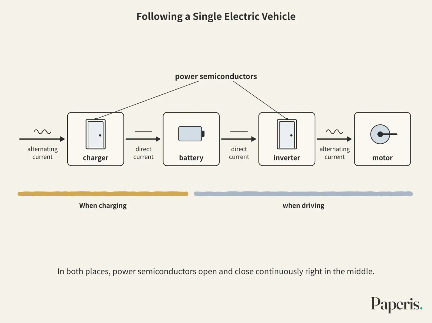
As of 2022, the most widely used power semiconductors in most commercial vehicles are a type of silicon switch. That trend has begun to shift with the introduction of wide-bandgap semiconductors (DOI: 10.1002/er.8581).
There is a study comparing silicon-carbide inverters and silicon inverters under the same standard driving conditions. Calculated using a loss model fitted from experiments, the largest loss of the silicon-carbide inverter was about one-third that of the silicon inverter, and the area of the semiconductor chip inside was half (DOI: 10.1109/apec.2018.8341204). A review paper combining multiple studies also highlights that silicon-carbide switches have the advantages of increasing efficiency in electric vehicles, packing more power into the same volume, and simplifying cooling systems (DOI: 10.1049/pel2.12524).
The same review also notes the trade-offs. Replacing a silicon switch with a silicon-carbide switch increases electromagnetic noise, the voltage spikes that momentarily surge can damage the motor's insulation, and cooling becomes trickier (DOI: 10.1049/pel2.12524). It is similar to how opening and closing a heavy door too forcefully makes the whole house rattle with a loud bang.
You can reduce the resulting electromagnetic noise by controlling how steeply you perform a single turn-on and turn-off operation. Here, steepness is different from how many times you open and close per second; the shorter the time it takes to turn on or off once, the steeper it is. There is a 2013 experiment that tested a 1200-volt-class device combination used in industrial motor drives. Much of what makes silicon-carbide switches better than silicon comes from turning them on and off more steeply, and pushing that steepness to the limit greatly increased electromagnetic noise. Even when they adjusted the turn-on and turn-off to match the same steepness as silicon and measured only the loss at that exact moment, the silicon-carbide combination had 70% less loss than the silicon combination (DOI: 10.1109/tpel.2013.2278919). Because this experiment measured switching loss rather than total loss, what was measured differs from the model calculations in the previous paragraph.
There are also examples on the charger side, which handles much smaller electricity. Power adapters for electronic devices are constantly demanded to be smaller and lighter. One study designed a 65-watt adapter that reduces conduction loss and switching loss using gallium-nitride switches, opening and closing on the scale of 1 million times per second (DOI: 10.1109/apec.2016.7468191). This device differs significantly from the hybrid vehicle converter we saw earlier in both the magnitude of the electricity it handles and the number of times it opens and closes per second. As much as losses are reduced, you can open and close more frequently, and opening and closing more frequently creates room to make components like coils inside the converter smaller (DOI: 10.1109/tia.2009.2027538).
Remaining Homework
Imperfections in silicon carbide crystals are remaining homework. Based on a 2020 review, defects inside the silicon carbide crystal and defects near the boundary where the switch's thin oxide film meets the silicon carbide greatly limit performance and reliability, and attempts to reduce these defects continue (DOI: 10.35848/1882-0786/abc787). Based on 2015 data, there was an evaluation that basic understanding of how silicon carbide's material properties and defects affect electricity, as well as device reliability, was still lacking (DOI: 10.7567/jjap.54.040103). How defects become a problem in making chips is covered in another part of this series, the one dealing with manufacturing.
Whether they hold up over long-term use is also homework. There is a 2014 experiment that purposely created conditions where a circuit was connected incorrectly and a large current poured in all at once. Even after just a few of these tests, the silicon carbide switch's structure that receives opening and closing signals broke down, while the side blocking voltage still held up. This was a worse result than similarly rated silicon devices (DOI: 10.1109/tpel.2014.2353417). A 2019 review noted that the durability and reliability of silicon carbide switches remain a major concern, especially in safety-critical applications (DOI: 10.1049/iet-pel.2019.0587). Because gallium nitride differs significantly from silicon and silicon carbide in its material, structure, and operating principles, it carries its own distinct stability and reliability problems (DOI: 10.1109/tpel.2023.3266365).
Price and packaging also remain. For power semiconductors grown with gallium nitride on silicon to sell widely, price, reliability, and ease of use are cited as problems that need to be solved (DOI: 10.1109/ted.2017.2657579). Traditional packaging methods that encase the chip have also acted as roadblocks preventing silicon carbide from realizing its full advantages (DOI: 10.24295/cpsstpea.2017.00017). Encasement of the chip and heat removal are covered in another part of this series, Packaging — A Chip Laid Face Down, a Three-Legged Race with Mismatched Strides.
The electromagnetic noise, motor insulation, reliability, and cooling problems seen in the previous section have kept silicon carbide switches from spreading widely in automobiles as of 2023, compared to mature silicon technology (DOI: 10.1049/pel2.12524). Research on packaging and driving methods to reduce these problems, as well as methods to increase durability, is continuing alongside them (DOI: 10.1049/pel2.12524; DOI: 10.1049/iet-pel.2019.0587). The new materials brought lower losses along with the homework of defects, reliability, and cost.
Instead of Changing the Door, You Hang Them in Combination
Sometimes materials are mixed and matched within a single converter. A study comparing DC-DC converters for hybrid vehicles tested an all-silicon combination, a combination pairing a silicon switch with a silicon carbide Schottky diode, and an all-silicon carbide combination side by side (DOI: 10.1109/tvt.2014.2323193).
Like the voltage-by-voltage map we saw earlier, where materials are used is divided by voltage, cost, and how long they have been proven in practice (DOI: 10.1109/tie.2019.2945299). Silicon and the new materials divide up their roles depending on the application.
The door analogy in this article breaks down from reality in three places. First, real power semiconductors have no moving door panels. Electrical signals create and then erase the paths for electricity to travel. Second, the "moment it is half open" describes the brief overlap between the voltage across the ends of the switch and the current passing through it during the transition between on and off. There is no tilted door panel anywhere, and the relationship between that overlap and switching loss is sketched here purely as a metaphor. Third, which door to hang is not decided by durability alone. Cost, defects, and how well it holds up over long-term use are also weighed.
Where to Explore Further
Power semiconductors are, after all, switches. How switches are turned on and off by electricity is covered in "A Transistor Is a Switch — A Tiny Faucet You Open and Close with Electricity". The terms voltage, current, and power can be explored further in "Voltage, Current, Power — What Goes All the Way Around Undiminished", and what alternating current is and why it is used in "Alternating Current and Frequency — A Giant Merry-Go-Round the Whole Country Pushes Together". The path electricity takes from the power plant to the wall outlet and the transformers that change voltage are found in "Transmission, Distribution, Transformers — The Road from Power Plant to Wall Outlet".
Why loss turns into heat and where that heat flows is covered in "Heat and Temperature — Water That Only Flows Downhill, a Pump That Lifts It Back Up", and the EV battery itself in "The Battery Cell — A Rocking Chair Between Two Electrodes". The power and heat issues of a single chip lead into "Why Did the Clock Stop at 4 GHz — Dark Silicon and the Power Wall".
Band gaps and diodes connect to "Semiconductors and the p-n Junction — An Empty Space in a Full Parking Garage, a Line Crossed Only One Way", defects and yield to "From Wafer to Chip — Stencils Laid Layer upon Layer, Squares Cut Out at the End", and wrapping the chip and extracting heat to "Packaging — A Chip Laid Face Down, a Three-Legged Race with Mismatched Strides".
Source Papers
- "Applications of wide bandgap semiconductors in electric traction drives: Current trends and future perspectives" (2025) — DOI: 10.1016/j.rineng.2025.104679 — Wide bandgap semiconductor drive units increase efficiency and reduce heatsink size, significantly boosting module power density (review article, paper-number-style page numbers — not a book review).
- "Comparison of SiC MOSFET‐based and GaN HEMT‐based high‐efficiency high‐power‐density 7.2 kW EV battery chargers" (2018) — DOI: 10.1049/iet-pel.2017.0467 — Built and compared identical 240VAC/7.2kW chargers using 650V SiC and GaN respectively; at the same efficiency, GaN is smaller, more efficient, and cheaper, while SiC has better thermal performance.
- "New FOM-Based Performance Evaluation of 600/650 V SiC and GaN Semiconductors for Next-Generation EV Drives" (2012) — DOI: 10.1109/access.2022.3174777 — Drive inverters handle DC/AC conversion between the battery and the motor, with SiC and GaN outperforming each other depending on temperature and switching frequency.
- "Material science and device physics in SiC technology for high-voltage power devices" (2015) — DOI: 10.7567/jjap.54.040103 — Power semiconductors are core components of power conversion systems, and fundamental understanding of SiC material properties, defects, and reliability remains insufficient.
- "Reliability and failure analysis in power GaN-HEMTs: An overview" (2017) — DOI: 10.1109/irps.2017.7936282 — GaN transistors for switching-mode converters experience critical conditions such as hard-switching moments where large current and voltage are applied simultaneously.
- "Comprehensive Efficiency, Weight, and Volume Comparison of SiC- and Si-Based Bidirectional DC–DC Converters for Hybrid Electric Vehicles" (2014) — DOI: 10.1109/tvt.2014.2323193 — Compared three combinations at 20kHz (all-Si, Si+SiC diode, and all-SiC) and explored the potential to reduce size and weight by increasing frequency and reducing capacitor and coil values.
- "SiC power devices — Present status, applications and future perspective" (2011) — DOI: 10.1109/ispsd.2011.5890778 — The main advantage of wide bandgap is the high critical electric field, enabling the design of switches with much lower both turn-on loss and switching loss.
- "The Loss Analysis and Efficiency Optimization of Power Inverter Based on SiC mosfets Under the High-Switching Frequency" (2020) — DOI: 10.1109/tia.2020.3045116 — Inverter losses increase linearly with switching frequency, mainly due to increased switching losses.
- "High-temperature electronics - a role for wide bandgap semiconductors?" (2002) — DOI: 10.1109/jproc.2002.1021571 — Silicon power devices become difficult to use above 200°C ambient temperature due to self-heating increasing junction temperature and leakage.
- "Design and Performance of a 200-kHz All-SiC JFET Current DC-Link Back-to-Back Converter" (2009) — DOI: 10.1109/tia.2009.2027538 — Link coils were large and heavy due to the low switching frequency of conventional high-voltage silicon devices, and raising the frequency with low-switching-loss SiC reduced their size and weight.
- "Silicon carbide benefits and advantages for power electronics circuits and systems" (2002) — DOI: 10.1109/jproc.2002.1021562 — Silicon has a narrow bandgap, low thermal conductivity, and switching frequency limits, while SiC and GaN achieve higher blocking voltage, frequency, and junction temperature through a wide bandgap and high breakdown electric field.
- "A Survey of Wide Bandgap Power Semiconductor Devices" (2013) — DOI: 10.1109/tpel.2013.2268900 — Wide bandgap semiconductors enable higher temperatures, voltages, and switching speeds than silicon, with SiC and GaN being the most promising in terms of properties, raw material availability, and process maturity.
- "University Physics Volume 3 — 9.5 Band Theory of Solids" (2016) — OpenStax University Physics Volume 3 9.5 — Electron energies in solids form bands with gaps between them.
- "Review of Silicon Carbide Processing for Power MOSFET" (2022) — DOI: 10.3390/cryst12020245 — SiC has a higher breakdown voltage, thermal conductivity, operating frequency, and operating temperature than silicon.
- "Review of Silicon Carbide Power Devices and Their Applications" (2017) — DOI: 10.1109/tie.2017.2652401 — SiC power devices operate at higher voltages, switching frequencies, and temperatures due to material advantages.
- "Current Status and Future Trends of GaN HEMTs in Electrified Transportation" (2020) — DOI: 10.1109/access.2020.2986972 — GaN offers higher efficiency and power density than silicon and makes passive components smaller, making systems lighter and more compact.
- "Gallium Nitride Power Devices: A State of the Art Review" (2023) — DOI: 10.1109/access.2023.3277200 — GaN power devices lag a few steps behind SiC in development, standardization, and power levels.
- "Performance and Reliability Review of 650 V and 900 V Silicon and SiC Devices: MOSFETs, Cascode JFETs and IGBTs" (2019) — DOI: 10.1109/tie.2019.2945299 — Silicon below 100V, SiC around 1kV and above for automotive, silicon devices above 4.5kV for the power grid, and no clear choice around 650V. GaN offers speed and integration, SiC high temperature and robustness, and silicon low cost and proven reliability.
- "The role of power device technology in the electric vehicle powertrain" (2022) — DOI: 10.1002/er.8581 — Silicon IGBTs are most widely used in commercial vehicles but are beginning to be replaced with the advent of wide bandgap devices.
- "High efficiency SiC traction inverter for electric vehicle applications" (2018) — DOI: 10.1109/apec.2018.8341204 — Using an experimentally calibrated loss model, a SiC inverter shows about 3 times lower peak loss and a 2 times smaller chip area than an IGBT inverter over standard driving cycles.
- "A review of silicon carbide MOSFETs in electrified vehicles: Application, challenges, and future development" (2023) — DOI: 10.1049/pel2.12524 — In electric vehicles, SiC offers efficiency, power density, and simplified cooling advantages, but has not yet been widely adopted due to EMI, reliability, motor insulation, and cooling issues.
- "An Experimental Investigation of the Tradeoff between Switching Losses and EMI Generation With Hard-Switched All-Si, Si-SiC, and All-SiC Device Combinations" (2013) — DOI: 10.1109/tpel.2013.2278919 — The top speed of SiC greatly increases EMI, but even at the same dv/dt, all-SiC has 70% less switching loss than all-Si.
- "Design consideration of MHz active clamp flyback converter with GaN devices for low power adapter application" (2016) — DOI: 10.1109/apec.2016.7468191 — Designed a MHz-class 65W adapter using GaN to reduce conduction and switching losses.
- "Defect engineering in SiC technology for high-voltage power devices" (2020) — DOI: 10.35848/1882-0786/abc787 — Defects such as oxide/SiC interface defects and stacking fault expansion severely limit the performance and reliability of SiC power MOSFETs.
- "Gate Oxide Reliability Issues of SiC MOSFETs Under Short-Circuit Operation" (2014) — DOI: 10.1109/tpel.2014.2353417 — A few short-circuit tests destroy the gate structure of SiC MOSFETs while drain-source still holds, worse than comparable grade silicon.
- "Review and analysis of SiC MOSFETs' ruggedness and reliability" (2019) — DOI: 10.1049/iet-pel.2019.0587 — The ruggedness and reliability of SiC MOSFETs remain major concerns, especially in safety-critical applications.
- "Stability, Reliability, and Robustness of GaN Power Devices: A Review" (2023) — DOI: 10.1109/tpel.2023.3266365 — GaN has distinct stability, reliability, and robustness issues because its material, structure, and physics differ from silicon and SiC.
- "GaN-on-Si Power Technology: Devices and Applications" (2017) — DOI: 10.1109/ted.2017.2657579 — Key challenges for commercializing GaN-on-Si are cost, reliability, and ease of use.
- "A Review of SiC Power Module Packaging: Layout, Material System and Integration" (2017) — DOI: 10.24295/cpsstpea.2017.00017 — Conventional device packaging is a limiting factor in fully exploiting the advantages of SiC.
Sources (29)
- Applications of wide bandgap semiconductors in electric traction drives: Current trends and future perspectivesDOI 10.1016/j.rineng.2025.104679
- Comparison of SiC MOSFET‐based and GaN HEMT‐based high‐efficiency high‐power‐density 7.2 kW EV battery chargersDOI 10.1049/iet-pel.2017.0467
- New FOM-Based Performance Evaluation of 600/650 V SiC and GaN Semiconductors for Next-Generation EV DrivesDOI 10.1109/access.2022.3174777
- Material science and device physics in SiC technology for high-voltage power devicesDOI 10.7567/jjap.54.040103
- Reliability and failure analysis in power GaN-HEMTs: An overviewDOI 10.1109/irps.2017.7936282
- Comprehensive Efficiency, Weight, and Volume Comparison of SiC- and Si-Based Bidirectional DC–DC Converters for Hybrid Electric VehiclesDOI 10.1109/tvt.2014.2323193
- SiC power devices — Present status, applications and future perspectiveDOI 10.1109/ispsd.2011.5890778
- The Loss Analysis and Efficiency Optimization of Power Inverter Based on SiC mosfets Under the High-Switching FrequencyDOI 10.1109/tia.2020.3045116
- High-temperature electronics - a role for wide bandgap semiconductors?DOI 10.1109/jproc.2002.1021571
- Design and Performance of a 200-kHz All-SiC JFET Current DC-Link Back-to-Back ConverterDOI 10.1109/tia.2009.2027538
- Silicon carbide benefits and advantages for power electronics circuits and systemsDOI 10.1109/jproc.2002.1021562
- A Survey of Wide Bandgap Power Semiconductor DevicesDOI 10.1109/tpel.2013.2268900
- University Physics Volume 3 — 9.5 Band Theory of Solids
- Review of Silicon Carbide Processing for Power MOSFETDOI 10.3390/cryst12020245
- Review of Silicon Carbide Power Devices and Their ApplicationsDOI 10.1109/tie.2017.2652401
- Current Status and Future Trends of GaN HEMTs in Electrified TransportationDOI 10.1109/access.2020.2986972
- Gallium Nitride Power Devices: A State of the Art ReviewDOI 10.1109/access.2023.3277200
- Performance and Reliability Review of 650 V and 900 V Silicon and SiC Devices: MOSFETs, Cascode JFETs and IGBTsDOI 10.1109/tie.2019.2945299
- The role of power device technology in the electric vehicle powertrainDOI 10.1002/er.8581
- High efficiency SiC traction inverter for electric vehicle applicationsDOI 10.1109/apec.2018.8341204
- A review of silicon carbide MOSFETs in electrified vehicles: Application, challenges, and future developmentDOI 10.1049/pel2.12524
- An Experimental Investigation of the Tradeoff between Switching Losses and EMI Generation With Hard-Switched All-Si, Si-SiC, and All-SiC Device CombinationsDOI 10.1109/tpel.2013.2278919
- Design consideration of MHz active clamp flyback converter with GaN devices for low power adapter applicationDOI 10.1109/apec.2016.7468191
- Defect engineering in SiC technology for high-voltage power devicesDOI 10.35848/1882-0786/abc787
- Gate Oxide Reliability Issues of SiC MOSFETs Under Short-Circuit OperationDOI 10.1109/tpel.2014.2353417
- Review and analysis of SiC MOSFETs' ruggedness and reliabilityDOI 10.1049/iet-pel.2019.0587
- Stability, Reliability, and Robustness of GaN Power Devices: A ReviewDOI 10.1109/tpel.2023.3266365
- GaN-on-Si Power Technology: Devices and ApplicationsDOI 10.1109/ted.2017.2657579
- A Review of SiC Power Module Packaging: Layout, Material System and IntegrationDOI 10.24295/cpsstpea.2017.00017