Paperis Articles
Packaging — A Chip Laid Face Down, a Three-Legged Race with Mismatched Strides
A die cut from a wafer cannot be used bare. Packaging encloses and protects it, connects it to the outside with fine wires or tiny solder bumps, and opens a path for heat to escape. Because materials expand by different amounts when heated, the joints between them wear out over time.
Your field's papers, as audio
Pick your fields and journals — Paperis summarizes the key papers and turns them into audio. Listen on your commute.
Start Paperis free →Packaging — A Chip Laid Face Down, a Three-Legged Race with Mismatched Strides
A Gray Piece on Your Palm
If you open a mobile phone, you will find a few black, flat rectangular components sitting on a green circuit board. What people commonly call a "chip" is this black rectangle. But the real body that does the calculation is a much smaller, thinner gray piece tucked inside it. The black rectangle is the part that wraps around that piece and connects it to the outside.
Let us imagine placing a freshly cut gray piece from the factory onto your bare hand. You cannot put it into a phone like this. There are three catches. First, it is thin and brittle, so it breaks if bumped, and it is fully exposed to the outside air and dust. Second, its tiny surface is lined densely with spots that need to be electrically connected to the outside, and they are too small and tight for you to touch wires to by hand. Third, when electricity flows in and it starts working, the piece heats up.
This article follows how those three problems are solved. It is about wrapping and protecting the piece, connecting it to the outside, and paving a way for heat to escape. And it goes all the way to why that work is appearing in the news so often these days.
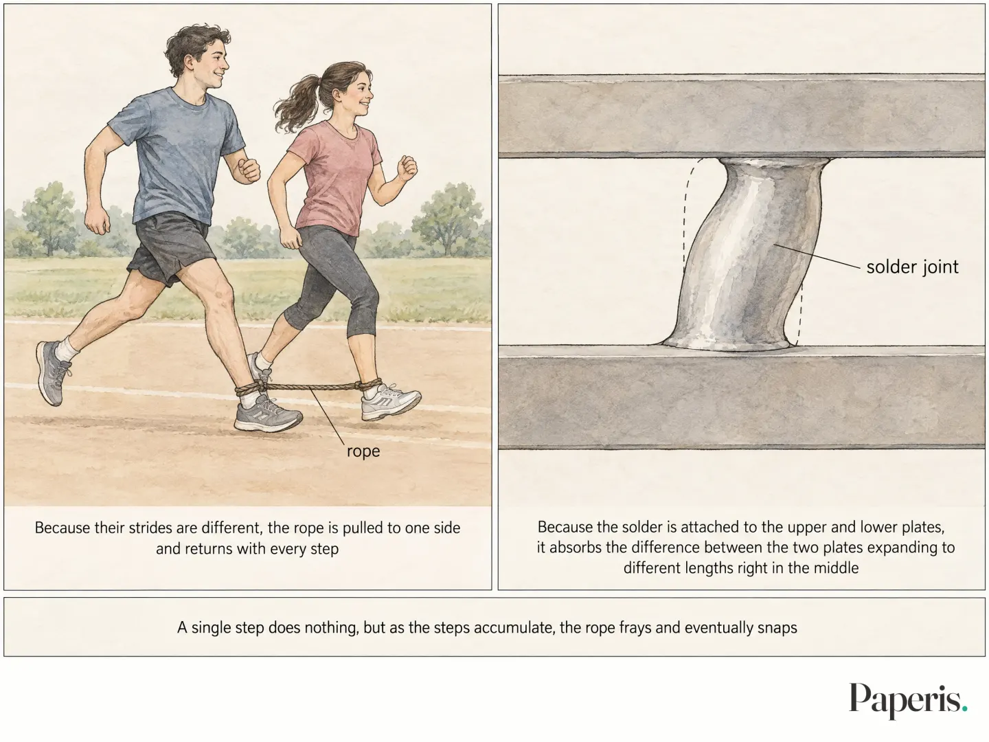
The guide image is the three-legged race at a sports day. It is a game where two people tie one ankle together with a rope and run as a pair, and if their strides differ, the tied strap gets pulled with every step. Where this image fits comes later.
Die and Package
The gray piece of material is a semiconductor. A semiconductor is a substance sitting halfway between a metal, which conducts electricity well, and glass, which hardly conducts it at all; under certain conditions, it either lets electricity through or blocks it. Chips are made from silicon, which is such a semiconductor. A wafer is a thin, round plate of silicon used to make chips. The same circuit is engraved like a checkerboard in many copies across a single wafer and then sliced out square by square. A die is a single piece of chip cut out from a wafer. The gray piece resting on your hand is the die. The process of engraving circuits and cutting them into dies is traced by the process-focused articles elsewhere in this series.
That component encasing the die has a name, too. The package is the entire assembly surrounding the die that protects it and connects it to the external circuitry. The black rectangle you see in mobile phones is the package. Packaging is the work of putting a die into a package, taking on the shared tasks of protecting the die, connecting it electrically to the outside, supplying electricity, and cooling the heat. A review of ceramic packaging for computers in the 1990s also groups packaging as the tasks of connecting the chip, supplying power, protecting it, and cooling it (DOI: 10.1111/j.1151-2916.1991.tb04320.x).
The first problem to be solved is problem number one: the problem of breakage and exposure. An encapsulant is the material that covers and envelops the die and its joints. The encapsulant protects the die from mechanical force, dielectric breakdown where electricity punctures insulation, chemical corrosion, and radiation such as alpha rays (DOI: 10.1109/tcpmt.2014.2337300). Thanks to the encapsulant, the die becomes an object that can be held in the hand, moved by machines, and attached to circuit boards.
The remaining two problems—namely, connecting and cooling—depend on what is used to connect the die to the outside world. There are broadly two ways to connect.
Connecting with Thin Wires
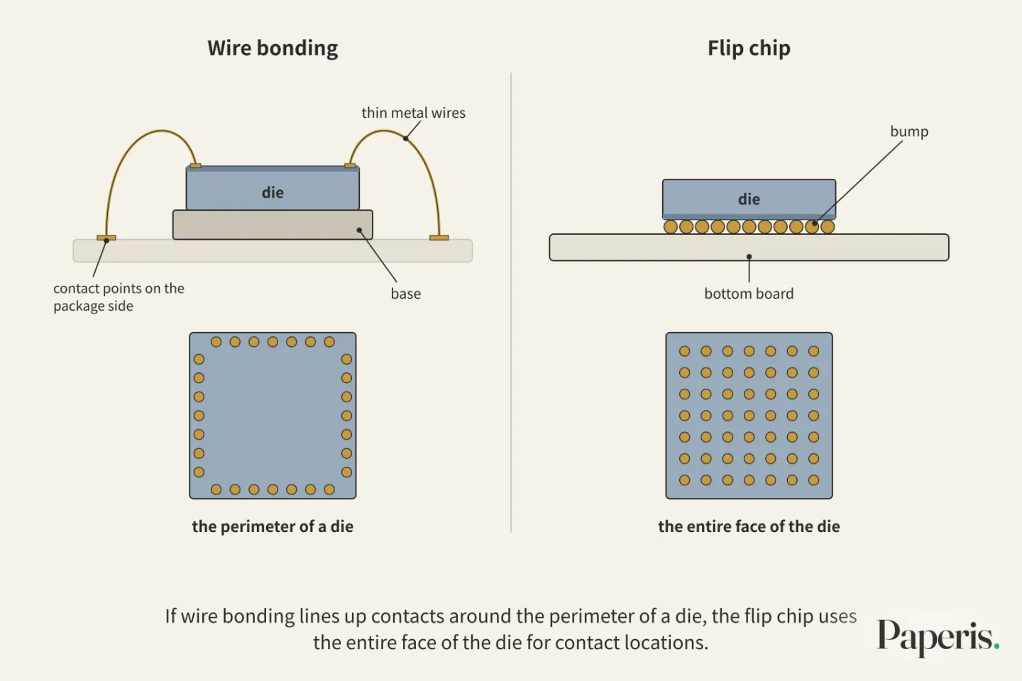
This is the method used for a long time. The die is seated on a base, and thin metal wires are hooked to each contact point on the die and stretched out to the contact points on the package side. Wire bonding is a method that connects the contact points of the die and the package one by one with thin metal wires.
There is a method of pressing the end of the wire against the contact point and attaching it with ultrasonic waves. When a 1977 study examined this with gold and aluminum wires, the two metals were bonded primarily by crushing deformation from being pressed rather than by heat or sliding (DOI: 10.1109/tphp.1977.1135225). This means that forcefully pressing and mashing the metals together accounts for the main share of the bonding strength.
The contact points to hook the wires to are usually arranged in a row along the edge of the die. In such an arrangement, the length of the die's perimeter limits the space available for placing contact points.
Flipping and Connecting
Another method flips the die. Flip chip is a method where the die is flipped so that the side with the circuitry faces downward, and the contacts on that side are attached directly to the bottom board. Between the flipped face and the bottom board, a small bump is wedged at each contact. A bump is a small protrusion formed by raising a round dome of metal, like solder, on top of a die's contact.
Solder is an alloy that melts at a relatively low temperature and then solidifies to bond metal to metal. Lead-containing solder was used in the past, but the electronics industry shifted to lead-free solder due to environmental concerns (DOI: 10.1146/annurev.matsci.38.060407.130253). The lead-free solders highlighted as promising by a 2005 study are all tin-rich alloys that melt between 210 degrees and 227 degrees Celsius (DOI: 10.1147/rd.494.0607). A solder joint is the spot where melted and solidified solder holds two metal surfaces together. Once the bumps melt and solidify, those spots become the solder joints.
A study that flip-chip bonded optical devices using solder bumps notes that this method creates practically an unlimited number of electrical connections at once and spreads those contacts across the chip surface as needed (DOI: 10.1109/ectc.1990.122163). Instead of connecting contacts one by one, multiple contacts are joined together in a single process of flipping and bonding. If wire bonding lines up contacts around the perimeter of a die, the flip chip uses the entire face of the die for contact locations. The space available to place contacts is much wider when using the entire surface than when lining them up on just a single edge row.
When the connecting method changes, the path for heat to escape changes as well. There is a prototype of a power component handling large currents where wire bonding lines were replaced with flip-chip bumps, sandwiching the component between two top and bottom boards and cooling it from both sides (DOI: 10.1109/6144.974963). With the top surface cleared of wires, heat could be exhausted in that direction too. This result is a test of a single prototype.
Because bumps are also paths where electricity travels, failures originate from electricity as well. Electromigration is a phenomenon where a long-flowing electric current pushes metal atoms to one side, causing voids to form and grow. The cross-section of a bump is roughly ten to a hundred times larger than the cross-section of the wiring inside the die, causing current to crowd to one side at the boundary where the narrow wiring transitions into the thick bump. In a bump, voids begin to form near that place where the current crowds, and once formed, a void spreads rapidly across the contact surface (DOI: 10.1063/1.1432443). The same research team concludes that designing bumps so that current spreads evenly inside them makes them withstand electromigration better and carry more current (DOI: 10.1063/1.1432443). This means the shape of a bump is part of its lifespan.
The Middle Plate
A die flipped over via flip chip usually does not sit directly on the circuit board of a phone; instead, another plate is placed between them. A package substrate is an intermediate plate sandwiched between the die and the circuit board, connecting the die's contact points to the circuit board. The contact points on the die are too densely packed for the circuit board to accept directly. The wiring inside the substrate spreads those dense contact points out into wider intervals, moving them to positions the circuit board can receive.
The substrate does more than just carry electricity. A 1990 review of ceramic packaging outlines that substrate materials must simultaneously meet requirements spanning thermal, mechanical, electrical, and dimensional precision (DOI: 10.1111/j.1151-2916.1991.tb04320.x). In the packages of power components that handle large currents, the substrate is also a material that supports the die while blocking electricity (DOI: 10.1002/advs.202524348).
This creates two layers of joints. There are bumps between the die and the substrate, and there are solder joints between the bottom of the package and the circuit board. One study placed the solder joints of a flip chip side by side with the joints of a package attached to a circuit board via solder balls, examining how they respond to heat, mechanical force, and vibration (DOI: 10.1109/96.544363). For a single die to work inside a phone, it must pass through two layers of solder joints, and both must survive.
A Three-Legged Race with Different Strides
Now we return to the third problem: heat. When you open a game on your mobile phone, the die warms up. While the die is hotter than its surroundings, heat escapes following that temperature difference—moving from the die, through the bumps and the substrate, toward the circuit board (OpenStax University Physics Volume 2 1.6). When you close the game, everything cools down again.
Then what happens to the warmed die and board? They grow a little larger. Thermal expansion is when an object's size or volume increases or decreases because its temperature changes. Even when heated by the same amount, how much they grow differs depending on the material (OpenStax University Physics Volume 2 1.3).
What does that difference do to the joint? In an assembly where the die is mounted directly onto a circuit board, the silicon die and the circuit board expand by vastly different amounts, creating severe force and twisting on the solder joint between them, which leads to fatigue failure (DOI: 10.1109/6144.974964). Because the solder is attached to the upper and lower plates, it absorbs the difference between the two plates expanding to different lengths right in the middle. Thermal fatigue is a failure where a joint is repeatedly twisted during cycles of heating and cooling until it finally cracks.
Translated to a three-legged race, it looks like this. The two people running with their ankles tied together are the die and the plate below it, the difference in how much their strides stretch is the difference in expansion, and the rope tying their ankles together is the solder joint. One heat-and-cool cycle is a single step. Because their strides are different, the rope is pulled to one side and returns with every step. A single step does nothing, but as the steps accumulate, the rope frays and eventually snaps. If a joint cracks and breaks, that contact point can no longer conduct electricity.
This problem is old. A paper published in 1969 already addressed how the shape and dimensions of solder joints and chips alter reliability amidst the thermal fatigue experienced while using a device (DOI: 10.1147/rd.133.0251). The industry measures in advance how many steps a joint can endure using accelerated temperature cycling tests, which intentionally repeat heating and cooling quickly (DOI: 10.1109/6144.974964).
Even within a single solder joint, the stride is not uniform. A tin crystal expands along one axis twice as much as it does within the plane perpendicular to it. In one study among joints subjected to temperature fluctuations, joints dominated by tin crystals whose high-expansion axis lay nearly parallel to the substrate surface failed earlier than neighboring joints. The failed joints showed the greatest difference in expansion between the solder and the substrate at the contacting interface. Viewed across the entire solder ball, the orientation of the crystals appeared random from one joint to the next (DOI: 10.1109/tcapt.2008.916835). This means that how fast a joint fatigues depends even on the grain of the material.
There are things other than heat that torment the joint. A 2004 research team noted that as portable devices increased, the failures to watch out for were shifting from fatigue caused by heating and cooling to breaking from drop impacts (DOI: 10.1109/ectc.2004.1320275). Temperature, vibration, and electromigration also affect joint reliability (DOI: 10.1080/14686996.2019.1640072). One review notes that about 70% of electronic device failures originate from the packaging process, and the vast majority of those are failures of the solder joints (DOI: 10.1080/14686996.2019.1640072).
The three-legged race illustration differs from reality in two ways. First, while runners can try to match each other's strides while running in a race, the plates on either side of a joint simply expand as they are heated without adjusting to each other. Making those adjustments must be done in advance during manufacturing. What can be chosen are the shape and dimensions of the joint and chip (DOI: 10.1147/rd.133.0251), as well as the bonded materials. A review examining high-temperature power packages notes that reliability can be increased by reducing the difference in expansion between bonded materials (DOI: 10.1109/tpel.2014.2357836). Second, an actual package with a substrate bound inside is tied together in multiple layers—die, bumps, substrate, solder, and circuit board—and each layer has a different stride.
Multiple Chips in One Package
The fact that putting multiple dies into a single package has become more common plays a big part in why packaging is in the news so often lately. Advanced packaging is a broad term for methods that place multiple dies side by side or stacked vertically within a single package, connecting them to work together like a single chip. As carving circuits more finely drives up costs, design timelines, and complexity, the industry turned toward bundling dies made separately by function into a single chip using advanced packaging, a review paper summarizes. That review notes that doing this helps mix and match dies made with different generations of processes and reuse them in different products, which helps lower design costs and raise yields (DOI: 10.3390/electronics9040670). This trend of fragmenting and attaching dies is covered in "They Chose Not to Make It One Chip — The Bill for Cutting It Apart".
There are also several ways to connect dies to one another. Flip-chip using solder bumps, methods of attaching them with heat and pressure without solder, and methods of directly bonding copper and insulating films are used together and compared (DOI: 10.1109/edr.2024.3501214). The last method is covered separately in "Nothing In Between — How Bonding Two Surfaces Directly Became the Center of the Process".
When stacking dies vertically, the bumps become much smaller. Microbumps are tiny metal pillars capped with solder that are sandwiched between two surfaces to connect chip to chip. The smaller the bumps get, the more the same current crowds into narrower paths and generates more heat. Accordingly, electromigration and thermal migration—where atoms move along temperature differences—noticeably shorten the lifespan of solder joints (DOI: 10.1016/j.matdes.2020.108726).
Stacking also traps heat. When dies are layered on top of each other, hot spots form everywhere, the degrees to which materials expand mismatch, and the paths for heat to escape narrow (DOI: 10.1038/s44172-026-00590-y). To put it in terms of a three-legged race, it is a match with more people tied together. The more ankles are tied, the more cords there are to watch out for. The story of stacking memory dies and attaching them next to processing chips is covered in "The Bottleneck Was Never Compute — Ten Years of Stacking Memory Beside the Processor", and the problem of the package's base board warping is covered in "If the Board Warps, Nothing Above It Helps — The Bill for a Glass Base and In-Package Light".
We place the gray piece from the beginning back onto our palm. This time, the piece is flipped upside down, placed on the substrate via bumps, covered with encapsulant, and attached to the cell phone's circuit board using solder beneath the substrate. The piece that used to break and stay exposed has gone inside the encapsulant, and the dense contact points that could not be held by hand have connected all the way to the circuit board via the bumps and the substrate's wiring. When you turn on a game, heat escapes toward the circuit board through the bumps and the substrate, and the joints placed along that path run a step of the three-legged race every time the game is turned on and off.
When we lay out these three problems again, we can see what packaging does. How many contact points to place and where, which path heat will escape through, and how many steps the joints can endure are decided at this stage. Packaging is the stage that largely determines how much of the performance a die is capable of producing can actually be drawn out and used. A review examining the packaging of optical devices and micro-mechanical components also calls packaging a core technology that draws out the functions and performance of components (DOI: 10.1109/jstqe.2011.2113171).
Where to Look Next
The process of dies being made on a wafer and cut out is continued in "From Wafer to Chip — Stencils Laid Layer upon Layer, Squares Cut Out at the End", and power components that handle large currents are covered in "Power Semiconductors — A Big Door That Never Stops Swinging, and the Heat of the Half-Open Moment".
The trend of bundling multiple dies into a single package is covered in "They Chose Not to Make It One Chip — The Bill for Cutting It Apart", methods of bonding two surfaces directly without bumps in "Nothing In Between — How Bonding Two Surfaces Directly Became the Center of the Process", methods of stacking and attaching memory in "The Bottleneck Was Never Compute — Ten Years of Stacking Memory Beside the Processor" and "Fetching Is Slower Than Computing — The Memory Bottleneck and HBM", and the base board of a package in "If the Board Warps, Nothing Above It Helps — The Bill for a Glass Base and In-Package Light". The paths through which heat travels and the basics of thermal expansion can be found in "Heat and Temperature — Water That Only Flows Downhill, a Pump That Lifts It Back Up".
Source Papers
- "Ceramic and Glass‐Ceramic Packaging in the 1990s" (1991) — DOI: 10.1111/j.1151-2916.1991.tb04320.x — An overview stating that computer packaging connects chips, supplies power, protects, and cools them, and that ceramic substrates carry thermal, mechanical, electrical, and dimensional precision demands.
- "Survey of High-Temperature Polymeric Encapsulants for Power Electronics Packaging" (2015) — DOI: 10.1109/tcpmt.2014.2337300 — A survey noting that encapsulation protects semiconductors from mechanical stress, dielectric breakdown, chemical corrosion, and alpha rays, and that high-temperature encapsulating materials are lacking.
- "The Ultrasonic Welding Mechanism as Applied to Aluminum-and Gold-Wire Bonding in Microelectronics" (1977) — DOI: 10.1109/tphp.1977.1135225 — Ultrasonic bonding of aluminum and gold wires attaches primarily through deformation mechanisms rather than heating or sliding.
- "Electromigration and Thermomigration in Pb-Free Flip-Chip Solder Joints" (2010) — DOI: 10.1146/annurev.matsci.38.060407.130253 — Environmental concerns led lead-free solders to replace lead solders, and electromigration and thermomigration pose serious reliability problems (emphasizing current crowding and Joule heating) in fine-pitch flip-chip bumps.
- "Microstructure and mechanical properties of lead-free solders and solder joints used in microelectronic applications" (2005) — DOI: 10.1147/rd.494.0607 — Promising lead-free solders are all tin-rich alloys with melting points of 210 to 227°C, recommended for flip-chip bumps and similar applications.
- "Self aligned, flip chip assembly of photonic devices with electrical and optical connections" (1990) — DOI: 10.1109/ectc.1990.122163 — Solder bump flip-chip assembly creates a virtually unlimited number of electrical connections all at once in the arrangement required on the chip surface (applied to photonic devices).
- "Double-sided cooling for high power IGBT modules using flip chip technology" (2001) — DOI: 10.1109/6144.974963 — An IGBT module prototype that replaced wire bonding with flip-chip bumps to enable double-sided component cooling.
- "Current-crowding-induced electromigration failure in flip chip solder joints" (2002) — DOI: 10.1063/1.1432443 — A bump cross-section is 10 to 100 times larger than the wiring, causing current to crowd at the contact boundary, where voids form and spread rapidly along the contact surface, and designs that spread current evenly enhance electromigration resistance.
- "Emerging Advanced Electronic Packaging Materials for Thermal Management in Power Electronics" (2026) — DOI: 10.1002/advs.202524348 — A review stating that substrate materials in the power module's thermal path handle mechanical support and electrical insulation.
- "Solder joint reliability of flip chip and plastic ball grid array assemblies under thermal, mechanical, and vibrational conditions" (1996) — DOI: 10.1109/96.544363 — An investigation examining the thermal, mechanical, and vibrational responses together with thermal fatigue of flip-chip and PBGA solder joints.
- "University Physics Volume 2 — 1.6 Mechanisms of Heat Transfer" (2016) — OpenStax University Physics Volume 2 1.6 — Heat transfers when a temperature difference exists.
- "University Physics Volume 2 — 1.3 Thermal Expansion" (2016) — OpenStax University Physics Volume 2 1.3 — Thermal expansion is size and volume change according to temperature, with the degree of expansion depending on material properties (coefficient of linear expansion).
- "Thermal cycling analysis of flip-chip solder joint reliability" (2001) — DOI: 10.1109/6144.974964 — Large thermal mismatch deformation between the silicon die and the circuit board generates high stress and strain in solder joints, causing fatigue failure, with fatigue strength evaluated through accelerated temperature cycling tests (finite element analysis).
- "Geometric Optimization of Controlled Collapse Interconnections" (1969) — DOI: 10.1147/rd.133.0251 — The mechanical reliability of solder joints under thermal fatigue conditions during machine use, and the effect of joint and chip shapes and dimensions on reliability.
- "Influence of Sn Grain Size and Orientation on the Thermomechanical Response and Reliability of Pb-free Solder Joints" (2008) — DOI: 10.1109/tcapt.2008.916835 — The thermal expansion coefficient of tin is twice as large along the c-axis as in the basal plane; joints dominated by crystals whose c-axis is nearly parallel to the substrate plane fail before their neighbors, damaged joints show the maximum solder-substrate thermal mismatch, and crystal orientation is random from joint to joint.
- "Effect of thermal aging on board level drop reliability for Pb-free BGA packages" (2004) — DOI: 10.1109/ectc.2004.1320275 — Author description that as the market shifts toward mobile devices, the primary failure mode is changing from thermal cycling fatigue to drop impact fracture, with Kirkendall voids as the main mechanism reducing strength.
- "Reliability issues of lead-free solder joints in electronic devices" (2019) — DOI: 10.1080/14686996.2019.1640072 — A review covering the effects of temperature, vibration, tin whiskers, and electromigration, noting that about 70% of electronic device failures originate in the packaging process, mostly as solder joint failures.
- "Survey of High-Temperature Reliability of Power Electronics Packaging Components" (2014) — DOI: 10.1109/tpel.2014.2357836 — Reducing the thermal expansion coefficient mismatch between assembled materials increases reliability, with encapsulation serving as the biggest constraint at high temperatures.
- "Chiplet Heterogeneous Integration Technology—Status and Challenges" (2020) — DOI: 10.3390/electronics9040670 — A review showing that rising process costs, design periods, and complexity have driven the industry toward bundling multiple dies with advanced packaging, helping mix dies from different process generations and raise yields.
- "A Review of Die-to-Die, Die-to-Substrate and Die-to-Wafer Heterogeneous Integration" (2024) — DOI: 10.1109/edr.2024.3501214 — A review comparing solder flip-chip, lead-free thermocompression, and copper/insulator hybrid bonding.
- "New challenges of miniaturization of electronic devices: Electromigration and thermomigration in lead-free solder joints" (2020) — DOI: 10.1016/j.matdes.2020.108726 — A review stating that as microbumps shrink in 3D integration, high current density and Joule heating cause electromigration and thermomigration to shorten solder joint lifespan.
- "Thermal management of 3-D heterogeneously integrated microelectronics: challenges and future research directions" (2026) — DOI: 10.1038/s44172-026-00590-y — A review stating that 3D stacking creates thermal challenges such as uneven power density, hotspots, thermal expansion mismatch, and narrowing heat dissipation paths.
- "Review of Packaging of Optoelectronic, Photonic, and MEMS Components" (2011) — DOI: 10.1109/jstqe.2011.2113171 — A review stating that packaging is a core technology drawing out component function and performance, connecting components and the environment through reliable joints.
Sources (23)
- Ceramic and Glass‐Ceramic Packaging in the 1990sDOI 10.1111/j.1151-2916.1991.tb04320.x
- Survey of High-Temperature Polymeric Encapsulants for Power Electronics PackagingDOI 10.1109/tcpmt.2014.2337300
- The Ultrasonic Welding Mechanism as Applied to Aluminum-and Gold-Wire Bonding in MicroelectronicsDOI 10.1109/tphp.1977.1135225
- Electromigration and Thermomigration in Pb-Free Flip-Chip Solder JointsDOI 10.1146/annurev.matsci.38.060407.130253
- Microstructure and mechanical properties of lead-free solders and solder joints used in microelectronic applicationsDOI 10.1147/rd.494.0607
- Self aligned, flip chip assembly of photonic devices with electrical and optical connectionsDOI 10.1109/ectc.1990.122163
- Double-sided cooling for high power IGBT modules using flip chip technologyDOI 10.1109/6144.974963
- Current-crowding-induced electromigration failure in flip chip solder jointsDOI 10.1063/1.1432443
- Emerging Advanced Electronic Packaging Materials for Thermal Management in Power ElectronicsDOI 10.1002/advs.202524348
- Solder joint reliability of flip chip and plastic ball grid array assemblies under thermal, mechanical, and vibrational conditionsDOI 10.1109/96.544363
- University Physics Volume 2 — 1.6 Mechanisms of Heat Transfer
- University Physics Volume 2 — 1.3 Thermal Expansion
- Thermal cycling analysis of flip-chip solder joint reliabilityDOI 10.1109/6144.974964
- Geometric Optimization of Controlled Collapse InterconnectionsDOI 10.1147/rd.133.0251
- Influence of Sn Grain Size and Orientation on the Thermomechanical Response and Reliability of Pb-free Solder JointsDOI 10.1109/tcapt.2008.916835
- Effect of thermal aging on board level drop reliability for Pb-free BGA packagesDOI 10.1109/ectc.2004.1320275
- Reliability issues of lead-free solder joints in electronic devicesDOI 10.1080/14686996.2019.1640072
- Survey of High-Temperature Reliability of Power Electronics Packaging ComponentsDOI 10.1109/tpel.2014.2357836
- Chiplet Heterogeneous Integration Technology—Status and ChallengesDOI 10.3390/electronics9040670
- A Review of Die-to-Die, Die-to-Substrate and Die-to-Wafer Heterogeneous IntegrationDOI 10.1109/edr.2024.3501214
- New challenges of miniaturization of electronic devices: Electromigration and thermomigration in lead-free solder jointsDOI 10.1016/j.matdes.2020.108726
- Thermal management of 3-D heterogeneously integrated microelectronics: challenges and future research directionsDOI 10.1038/s44172-026-00590-y
- Review of Packaging of Optoelectronic, Photonic, and MEMS ComponentsDOI 10.1109/jstqe.2011.2113171