
Paperis Articles
DRAM and NAND — Writing in Water That Dries, Writing in Stone That Must Be Ground Away
DRAM holds charge in a tiny capacitor in every cell. It answers quickly, but the charge leaks and must be topped up without rest. NAND locks charge in a spot enclosed by insulating layers so it survives power-off, but rewriting means erasing a whole block, and every write and erase wears the cell a little.
Your field's papers, as audio
Pick your fields and journals — Paperis summarizes the key papers and turns them into audio. Listen on your commute.
Start Paperis free →DRAM and NAND — Writing in Water That Dries, Writing in Stone That Must Be Ground Away
Memories in a Drawer and Memories That Never Rest
When you take a USB memory stick that you put in a drawer a few months ago and plug it into a computer, the files you stored back then open just fine. During all that time, electricity never flowed into that small stick even once. At the same time, inside a powered-on computer, the opposite happens. The memory used while working must have its contents refilled multiple times every single second while electricity flows just so it does not get forgotten.
The part that survived without electricity inside the USB memory is NAND, and the side that refills without resting is DRAM. This article follows how NAND and DRAM hold onto information inside their chips in their own ways, and therefore what they gain and what they give up. Why a computer has two separate types of memory slots was covered in "CPU and Memory — A Desk That Gets Cleared, Library Stacks That Stay", and this article looks inside the chips that go into those two slots.
We take two pictures as guides. Writing on a park stone floor with a water brush gets written the moment the brush touches, but dries and disappears in a few minutes. Writing carved into stone takes effort to carve, but remains for a long time even without someone guarding it. DRAM resembles the water writing, and NAND resembles the writing carved into stone.
The Compartment That Holds Memories
Memory is a chip that holds data to be used for computation and hands it out when needed. Both DRAM and NAND are memory chips made of silicon. A semiconductor is a material halfway between a metal that conducts electricity well and glass that barely conducts it at all, where electricity can either pass through or be blocked depending on the conditions. Silicon is such a material.
The data that memory holds is ultimately a long string of 0s and 1s. A bit is the smallest unit of information, representing either a 0 or a 1. Even a single photo is broken down and held as a vast number of bits inside the chip. A cell is the smallest compartment inside a memory chip that holds a bit. In a DRAM chip, the cells line up densely in matching rows and columns (OpenStax Introduction Computer Science 5.5).
DRAM and NAND differ in the way they trap bits in these compartments, and that difference shows when the electricity is cut off. DRAM is memory that holds data while a computer is working, and the contents it holds vanish when the power goes off. Volatility is the property where stored contents disappear when the power is cut. One of the reasons DRAM has taken charge of memory while work is ongoing is that the waiting time until it hands over data is short (DOI: 10.1109/tc.2015.2417540).
NAND flash is memory whose contents remain even when the power is turned off, where an entire block must be erased at once before writing anew. It is called NAND for short. Non-volatility is the property where stored values remain intact even when the power is cut.
NAND is a memory chip used for storage devices. A storage device is a component that keeps programs and data stored for a long time so that the contents remain intact even when the power is turned off. NAND is the main storage that holds photos and apps in mobile devices (DOI: 10.1002/adma.202200659). An SSD is a storage device containing multiple NAND chips together with a controller chip that manages them. It is also widely used as a laptop's storage device. The chips for storing and the circuit that handles those chips are the two parts of an SSD. Flash memory goes into both an SSD and the USB memory from the opening scene, and the flash memory in an SSD uses the NAND method (OpenStax Introduction Computer Science 5.5).
The two positions trade off different things. DRAM used as main memory is fast but volatile, while an SSD used as storage is slow but keeps its contents even when turned off, is cheaper, and holds a larger capacity (OpenStax Introduction Computer Science 5.5). Where that trade-off begins inside the cell is the question of this article.
DRAM — Water Writing Overwritten Before It Dries
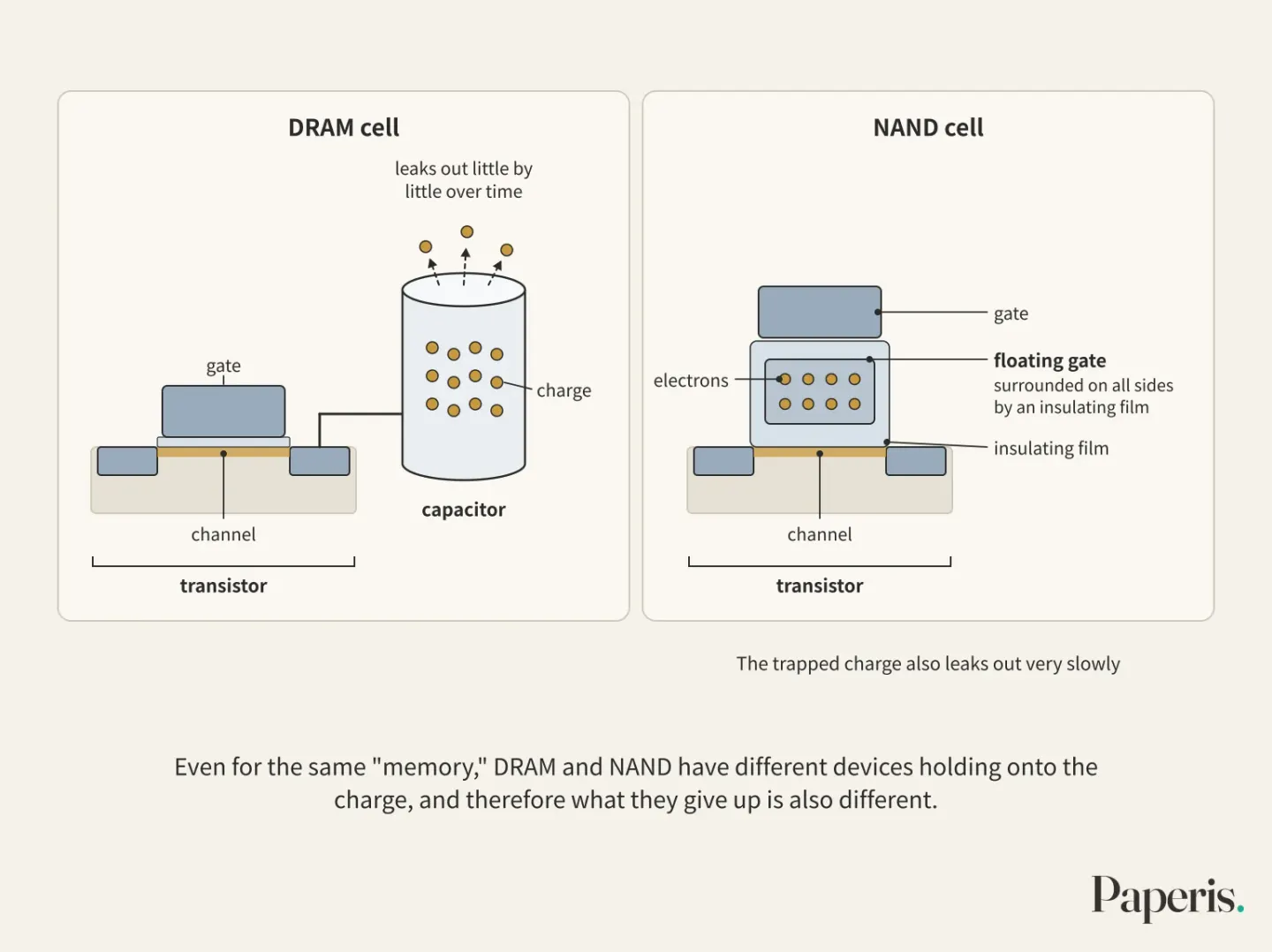
A single DRAM cell contains two components. They are one transistor and one capacitor, and data is stored in the capacitor (DOI: 10.1002/admt.202200878). A transistor is a tiny switch turned on and off by electricity. In the cell, it is responsible for opening and closing the path leading to the capacitor.
What is stored in the capacitor is electric charge. Electric charge is the amount of electricity an object carries. When electrons, which are tiny particles carrying a negative electric charge, gather in one place, a negative charge accumulates there. A capacitor is a component that collects and stores electric charge. A DRAM cell represents a single bit depending on whether electric charge is stored in the capacitor or not (OpenStax Introduction Computer Science 5.5). A single stroke painted with a water brush on a stone floor is the charge stored in a single cell's capacitor.
The charge stored in the capacitor leaks out little by little over time, and if left alone, the data is eventually lost (DOI: 10.1145/2508148.2485928). This is like water writing drying on a stone floor in the sunlight. That is why DRAM has a hand that rewrites. Refresh is the operation in which DRAM periodically reads and refills the stored contents so that it does not lose its values. According to a 2017 study, the standard at the time was to refresh all cells once every 64 milliseconds. That is a little over fifteen times a second (DOI: 10.1145/3079856.3080242).
The reason it is refilled so often is that the retention time varies greatly from cell to cell. The time a cell retains data ranges widely from a few milliseconds to several minutes, and the refresh interval is set to the very end of that distribution (DOI: 10.1145/3079856.3080242). A single cell that leaks the fastest determines the refresh speed for the entire chip, and since most cells last much longer than that, a significant portion of the refreshes are not actually necessary (DOI: 10.1145/2366231.2337161). This is like a person holding a water brush walking around the entire floor based on the letter that dries the fastest.
Therefore, methods of varying the refresh interval according to the time a cell lasts have also been researched (DOI: 10.1145/2366231.2337161). To do this, the retention time of each cell must be measured in advance, but for some cells, the retention time changes sometimes without warning, and it also varies depending on the values stored in other cells (DOI: 10.1145/2508148.2485928).
Refresh costs value. Energy is consumed during the refilling, and read and write requests coming in during that time must wait. As chips become larger and faster, this burden also grows (DOI: 10.1109/tc.2015.2417540).
Now let's look at the moment the power turns off in a single cell. When the power is cut, the refresh also stops. Without a hand to refill it, the charge in the capacitor leaks out, and the stored bit disappears. This is like the writing drying up completely on a stone floor after the person with the water brush has left. DRAM is a memory that has a short waiting time, but must be refilled without rest because the stored charge leaks.
NAND — Charge Locked in a Space Sealed on All Sides
A NAND cell has no separate capacitor. A single transistor holds memory on its own, and data is written onto the threshold at which that transistor turns on (DOI: 10.1109/jsac.2016.2603608). Let us take a closer look inside the transistor. The detailed structure is covered in "A Transistor Is a Switch — A Tiny Faucet You Open and Close with Electricity".
The channel is the path through which electric current passes between both ends of a transistor. This path is opened and closed by voltage. Voltage is the difference that causes electricity to flow between two points, measured in units called volts.
Opening and closing the channel is a piece placed on top of it. The gate is a piece placed over the channel with a thin film in between, and the voltage applied to it opens and closes the channel. The threshold voltage is the voltage at which the transistor starts to turn on when applied to the gate.
In the transistor of a NAND cell, another piece is wedged between the gate and the channel, and its perimeter is wrapped in a film that barely conducts electricity. The insulating film is a thin film through which electricity hardly flows. The floating gate is an electrically conductive piece wedged between the gate and the channel, surrounded on all sides by an insulating film so that it is not connected to anything anywhere. A 2003 primer noted that NAND cells are also based on such floating-gate transistors (DOI: 10.1109/jproc.2003.811702).
When writing, a high voltage is applied to the cell (DOI: 10.1109/hpca.2017.61) to push electrons across the thin insulating film into that piece. The electrons that enter are blocked by the surrounding insulating film and cannot escape, which changes the threshold voltage of that transistor. When reading, a predetermined reference voltage is applied to the cell (DOI: 10.1109/hpca.2018.00050), and whether the threshold voltage lies on one side or the other is determined by whether the transistor turns on. It is like carving letters into stone. It takes effort to carve, but the carved letters remain even after the person holding the water brush leaves.
There is one more way to trap electrons. Charge trap is a method of trapping electrons in an insulating film that has the property of holding onto electrons, instead of using an electrically conductive piece. A structure in which three layers of insulating film are stacked and charges are held in the middle layer is an example (DOI: 10.1063/1.1897431). The two methods differ in the materials used and the challenges to be solved, and a 2022 review article summarized those challenges focusing on charge trap NAND (DOI: 10.1002/adma.202200659). Whether it is a floating gate or a charge trap, NAND retains its memory even when the power is turned off because it traps electric charges in a space surrounded by an insulating film.
Rewrite It by Replacing the Whole Thing
Let us say you edit and save a single line in a notes app. NAND does not overwrite the cell where that line was in place. It writes the edited content anew into an empty space and leaves the old content behind as obsolete (DOI: 10.14778/2536360.2536372). This is because in NAND, you cannot write directly back into a spot that has already been used once (DOI: 10.1109/smartcomp.2014.7043841).
A block is a group of cells that are erased all at once in NAND. Flash memory is organized in units called pages, and a block is a collection of several pages (OpenStax Introduction Computer Science 5.5). When writing, you write line by line among them, but when erasing, you wipe out the block as a whole. You cannot erase just a single character carved into a stone tablet. To make a correction, you have to grind away an entire stone tablet and carve it anew, so for now you carve the new text in a blank spot beside it and treat the old text as discarded.
Empty spaces eventually run out. Garbage collection is the task of clearing away obsolete old data to create empty blocks that can be used again. This cleanup takes a lot of time, often becoming a bottleneck that drags down the speed of NAND storage devices (DOI: 10.1109/smartcomp.2014.7043841). Doing the cleanup also brings along the burden of writing more inside the chip than what the user intended to write (DOI: 10.1145/3456727.3463784). How much free space you leave behind and this write burden are in a trade-off relationship with each other (DOI: 10.14778/2536360.2536372). In NAND, rewriting is a combination of writing anew and a later whole-block erase, and that cleanup work makes writing heavy.
A Stone Tablet Damaged Every Time It Is Ground Down
A stone tablet becomes a little rougher on the surface every time it is ground down. NAND cells also suffer a little damage every time they are written to and erased, which is why there is a limit to the number of write cycles they can withstand (DOI: 10.1109/hpca.2018.00050). Write endurance is the value indicating how many write and erase cycles a cell can withstand. As one form of that damage, repeating writes and erasures can cause charge to get trapped and accumulate in the film on the channel, which can raise the threshold voltage of the cell (DOI: 10.1109/tdmr.2004.836721). When measuring multiple cells together, as the number of write and erase cycles increases, the distribution of threshold voltages shifts to one side and spreads out widely (DOI: 10.7873/date.2013.266). This is like how letters carved on a stone tablet with a roughened surface become harder to read.
The exact number of cycles it takes to wear out is not a fixed value. In the introduction of a 2014 paper, the authors cited a general figure that flash cells typically wear out after a few thousand write and erase cycles (DOI: 10.5555/2591305.2591311). When the same paper measured two commercial devices, differences in writing methods and small manufacturing variations caused some cells to wear out much faster than others, and the authors projected that this difference would grow larger in future process generations (DOI: 10.5555/2591305.2591311). The lifespan of NAND has grown shorter as cells have been made smaller (DOI: 10.1109/hpca.2018.00050). Meanwhile, some of the damage heals itself during the resting periods between writing and erasing (DOI: 10.1109/hpca.2018.00050).
There is a dedicated chip that handles this wear. This is the SSD controller we saw earlier. As cells have been made smaller and store more bits per cell, the values read from the cells have become blurry, and the controller has come to incorporate various techniques to correctly interpret those blurry values and fix errors (DOI: 10.1109/jproc.2017.2713127). Wear leveling is a design that distributes writes evenly across cells so that a single spot does not wear out first. Because the number of write cycles a cell can withstand is very small compared to hard disks, wear leveling is indispensable for NAND management (DOI: 10.1109/smartcomp.2014.7043841). This is like taking turns using multiple stone tablets so that only one piece does not wear out first. Write endurance counts the number of writes and erasures a single cell can withstand. Modified content is newly written to an empty space (DOI: 10.14778/2536360.2536372), and wear leveling distributes those writes across multiple locations (DOI: 10.1109/smartcomp.2014.7043841).
Evaluations exist on how to interpret the stated endurance. A 2019 paper discussing the lifespan of 3D NAND reported that manufacturers typically define endurance as the maximum number of cycles that the weakest block can withstand, while the error rate of most blocks does not reach the allowable limit even at that point; the authors evaluated that the lifespan of blocks goes underutilized because of this conservatively set endurance (DOI: 10.1109/access.2019.2909567).
Even words carved in stone are not permanent. How long trapped charge remains is one of the main reliability issues of NAND (DOI: 10.1109/jproc.2003.811702). In 3D NAND, a phenomenon was observed where the number of errors inside the chip rapidly increased for several hours after writing due to leaking charge, and the same study also proposed a method to reduce these errors by adjusting the reference voltage during reading to match how long ago the data was written (DOI: 10.1145/3224432). Temperature also changes the rate at which charge leaks (DOI: 10.1109/hpca.2018.00050). NAND actually wears out the more it is written to and erased, and trapped charge also leaks out little by little; the wearing speed varies from cell to cell, so the controller shares that difference and reads by correcting errors.
Multiple Bits in a Single Compartment
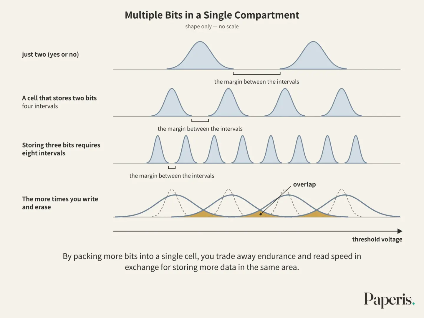
Imagine carving a stone tablet where you divide the depth of a single carved compartment into four levels. That compartment now holds one of four states instead of just two (yes or no). NAND flash does the same thing using the amount of trapped charge. A multi-level cell is a method that divides the amount of charge trapped in a single cell into multiple levels, storing two or more bits. A cell that stores two bits divides the range of threshold voltages into four intervals (DOI: 10.1109/hpca.2017.61). This makes it possible to pack nearly twice as much data into the same chip size, lowering the cost per bit (DOI: 10.1109/jproc.2003.811702). Storing three bits requires eight intervals.
The price paid is the margin between the intervals. As cells have been made smaller and the number of steps increased, the number of electrons representing a single step has decreased, and the interference of neighboring cells shaking one another has grown (DOI: 10.1109/jproc.2017.2713127). When the threshold voltage distribution—which spreads more widely the more times you write and erase—overlaps with a neighboring interval, that overlap becomes the cause of reading errors (DOI: 10.1109/irps.2019.8720454). Therefore, storing multiple bits in a single cell creates new challenges in write endurance and read/write speed (DOI: 10.1145/3352460.3358323). Because the process of changing the reference voltage and re-reading the same spot to find the correct value happens more frequently, reads can become noticeably slower (DOI: 10.1145/3445814.3446719). The more densely divided the depth steps on a stone tablet are, the more easily a slight roughness on the surface leads to misreading the depth. By packing more bits into a single cell, you trade away endurance and read speed in exchange for storing more data in the same area.
When You Can No Longer Draw Smaller
A nanometer is 1 billionth of a meter. NAND flash memory, which had been drawn as cells on a flat surface, had shrunk to around 15 nanometers by design standard around 2013 (DOI: 10.1002/adma.202200659). Researchers at one manufacturer wrote that as dimensions decreased, interference between neighboring cells grew larger and drawing circuits also became harder (DOI: 10.1109/jssc.2015.2474117). So NAND changed direction. 3D NAND is NAND where cells are stacked vertically layer upon layer instead of being drawn smaller on a flat surface. Doing this can increase storage density with much less strain on the manufacturing process (DOI: 10.1145/3224432). It was first reported that 3D NAND used charge trap cells, and devices using 3D floating gates also came out (DOI: 10.1109/isscc.2016.7417947). Since there was no more land to spread stone tablets wider sideways, they began stacking them upward.
As of 2022, NAND stacked to 176 layers was on the market, and as the layers increase, managing the stress the film receives and carving out deep holes become difficult (DOI: 10.1002/adma.202200659). The same review article projected that because of the limit allowed by the total chip thickness, there would likely be an upper bound of around 400 to 500 layers for what can be stacked (DOI: 10.1002/adma.202200659). There are also gains from stacking layers. A 2019 paper wrote that 3D NAND has a much larger capacity and better durability than the latest flat NAND (DOI: 10.1109/irps.2019.8720454). Instead, new causes of errors not seen in flat NAND also appeared, such as the phenomenon where the average error rate varies greatly from layer to layer (DOI: 10.1145/3224432).
DRAM faced the same wall. As cells become smaller, it becomes important for capacitors to hold charge generously, and DRAM has changed capacitor structures and insulator materials to maintain the amount stored even in narrowed spaces (DOI: 10.1002/admt.202200878). A 2008 study wrote that even if cells shrink, the amount the capacitor must hold does not decrease, so if miniaturization continues, materials that allow holding more must eventually be used, and the film found by that study also had a very small amount of leaking charge (DOI: 10.1002/adma.200701085).
A 2023 conference paper wrote that DRAM, which has increased density by shrinking transistors and capacitors together, faces growing process and reliability challenges if these devices are continued to be shrunk further. The same paper discussed opportunities and challenges, stating that DRAM could also choose a method of stacking cells upward like NAND (DOI: 10.23919/vlsitechnologyandcir57934.2023.10185290). Before the same wall, NAND took the path of stacking layers upward, and DRAM has walked the path of maintaining what the capacitor holds in narrowed compartments.
Back Again, In Front of the USB Drive in the Drawer
We can now view the first two scenes through the eyes of a cell. In the DRAM of a turned-on computer, the charge in the capacitors leaks constantly, and refresh refills it many times a second. In the NAND of the stick in the drawer, electrons trapped inside an insulating film stayed put even without electricity.
The two memories trade different things for one another. DRAM has a short wait time, but constantly refills the leaking charge. NAND stays even when turned off, but requires high voltage when written, clears block by block when fixed, and wears out the more it is written and cleared. Even for the same "memory," DRAM and NAND have different devices holding onto the charge, and therefore what they give up is also different.
The metaphor of writing on water and carving in stone also has its limits. A cell does not have the shape of a letter, only the amount of charge. The wearing out of a NAND cell is a matter of charge getting caught and piling up on the film and damaging the film, so nothing is chiseled away like a stone slab. And unlike letters carved in stone, the trapped charge also leaks out very slowly.
Where to Look Next
Why memory and storage are separate is in "CPU and Memory — A Desk That Gets Cleared, Library Stacks That Stay", and why the road carrying data from DRAM to the processor gets jammed is in "Fetching Is Slower Than Computing — The Memory Bottleneck and HBM". How the transistor inside a DRAM cell opens and closes its path can be seen in "A Transistor Is a Switch — A Tiny Faucet You Open and Close with Electricity". The race to find new memory that needs no refresh or keeps data when turned off is covered in "Next-Generation Memory — The DRAM Wall and the Race for a "Dream Memory"". The earlier 2022 review also proposed that a new storage method using ion movement could overcome the inherent problems of flash (DOI: 10.1002/adma.202200659).
The work of depositing and etching thin films can be seen in "From Wafer to Chip — Stencils Laid Layer upon Layer, Squares Cut Out at the End". Once you know that work, it becomes clearer why the layers and deep holes of 3D NAND are difficult. How electrons move inside a semiconductor is covered by "Semiconductors and the p-n Junction — An Empty Space in a Full Parking Garage, a Line Crossed Only One Way". Just how many layers 3D NAND can be stacked to, and whether DRAM will also be stacked upward, has not been decided yet.
Source Papers
- "Introduction to Computer Science — 5.5 Memory Hierarchy" (2024) — OpenStax Introduction Computer Science 5.5 — Main memory DRAM is volatile and fast, storage SSDs are non-volatile, slow, cheap, and high capacity, thumb drives and SSDs use flash memory, flash is organized into pages and blocks, memory cells are arranged in rows and columns.
- "DRAM Refresh Mechanisms, Penalties, and Trade-Offs" (2015) — DOI: 10.1109/tc.2015.2417540 — DRAM is used as main memory due to short latency and high density (comparison among main memory candidates), refreshes are a burden on performance and power, and become greater as chips get larger and faster.
- "Review of Semiconductor Flash Memory Devices for Material and Process Issues" (2022) — DOI: 10.1002/adma.202200659 — V-NAND is the primary storage of mobile devices, planar scaling reached down to about 15 nm based on 2013 designs, 176 layers have been commercialized, film stress and deep hole etching are challenges, chip thickness points to a 400 to 500 layer upper limit, reviews charge-trap based flash, and proposes ion-based new storage devices.
- "Toward Advanced High‐k and Electrode Thin Films for DRAM Capacitors via Atomic Layer Deposition" (2022) — DOI: 10.1002/admt.202200878 — A DRAM cell consists of one transistor and one capacitor, data is in the capacitor, securing sufficient capacitance becomes important as cells get smaller, progress on both structural and material fronts.
- "An experimental study of data retention behavior in modern DRAM devices: implications for retention time profiling mechanisms" (2013) — DOI: 10.1145/2508148.2485928 — DRAM cells hold data with a capacitor's charge and lose data as that charge leaks away, so a refresh is needed, observed data pattern dependency and unpredictably varying retention times across 248 chips.
- "The Reach Profiler (REAPER): Enabling the Mitigation of DRAM Retention Failures via Profiling at Aggressive Conditions" (2017) — DOI: 10.1145/3079856.3080242 — Cell retention times range from milliseconds to several minutes, and all cells are refreshed every 64 ms tailored to the tail of the distribution.
- "RAIDR: Retention-Aware Intelligent DRAM Refresh" (2012) — DOI: 10.1145/2366231.2337161 — Refresh speed is determined by the fastest leaking cell and most cells last much longer, making frequent refreshes unnecessary (numerical values of the proposed technique are not used in this article).
- "Enabling Accurate and Practical Online Flash Channel Modeling for Modern MLC NAND Flash Memory" (2016) — DOI: 10.1109/jsac.2016.2603608 — Flash cells hold data using the threshold voltage of a floating gate transistor.
- "Introduction to flash memory" (2003) — DOI: 10.1109/jproc.2003.811702 — Flash cells are floating gate MOS transistors (NAND shares the same concept), charge retention and endurance are major reliability issues, multi-level nearly doubles density for the same chip size, lowering cost per bit.
- "Vulnerabilities in MLC NAND Flash Memory Programming: Experimental Analysis, Exploits, and Mitigation Techniques" (2017) — DOI: 10.1109/hpca.2017.61 — High voltages are applied when writing to cells, MLC divides the threshold voltage range into four states to hold two bits.
- "HeatWatch: Improving 3D NAND Flash Memory Device Reliability by Exploiting Self-Recovery and Temperature Awareness" (2018) — DOI: 10.1109/hpca.2018.00050 — Lifespan has decreased due to miniaturization, write counts are limited because of damage from each write and erase while some self-recovery occurs during rest, temperature affects the rate of charge leakage, and read reference voltage is the voltage applied to a cell during a read.
- "Charge-trapping device structure of SiO2∕SiN∕high-k dielectric Al2O3 for high-density flash memory" (2005) — DOI: 10.1063/1.1897431 — A triple-layer charge trap structure (SANOS) consisting of tunnel oxide, nitride, and blocking oxide.
- "Improving flash write performance by using update frequency" (2013) — DOI: 10.14778/2536360.2536372 — Flash is inefficient at in-place updates, so the FTL uses a method of writing newly to a different location, trading off free space and write overhead.
- "Garbage collection and wear leveling for flash memory: Past and future" (2014) — DOI: 10.1109/smartcomp.2014.7043841 — Garbage collection is necessary and time-consuming, becoming a bottleneck because once written data cannot be overwritten immediately, and wear leveling is essential since cells endure far fewer writes than hard disks.
- "Constructing Large, Durable and Fast SSD System via Reprogramming 3D TLC Flash Memory" (2019) — DOI: 10.1145/3352460.3358323 — Multiple bits per cell pose challenges for endurance and access latency.
- "Reducing write amplification in flash by death-time prediction of logical block addresses" (2021) — DOI: 10.1145/3456727.3463784 — SSDs cannot perform in-place updates, carrying the burden of garbage collection and write amplification.
- "Wear unleveling: improving NAND flash lifetime by balancing page endurance" (2014) — DOI: 10.5555/2591305.2591311 — The introduction states that flash cells typically wear out after thousands of write-erase cycles, demonstrates in two commercial devices that write patterns and process variation cause some cells to wear out much faster, and concludes this variation will grow in future process generations.
- "Flash EEPROM Threshold Instabilities due to Charge Trapping During Program/Erase Cycling" (2004) — DOI: 10.1109/tdmr.2004.836721 — Repeated write and erase cycles can trap charges above the channel, raising the threshold voltage.
- "Threshold Voltage Distribution in MLC NAND Flash Memory: Characterization, Analysis and Modeling" (2013) — DOI: 10.7873/date.2013.266 — Threshold voltage distributions shift to the right and widen as write-erase counts increase (measured on 2Y-nm MLC chips).
- "RBER-Aware Lifetime Prediction Scheme for 3D-TLC NAND Flash Memory" (2019) — DOI: 10.1109/access.2019.2909567 — Manufacturers define endurance by the maximum write-erase cycles of the weakest block, but most blocks do not reach the allowable error rate at that point, leading the authors to evaluate that conservatism leaves lifespan unused.
- "Error Characterization, Mitigation, and Recovery in Flash-Memory-Based Solid-State Drives" (2017) — DOI: 10.1109/jproc.2017.2713127 — Miniaturization and multi-level design have reduced the number of electrons per cell and increased inter-cell interference, worsening reliability, and SSD controllers possess various techniques (interference mitigation, optimal sensing, error correction, recovery) to correctly interpret blurred values.
- "Improving 3D NAND Flash Memory Lifetime by Tolerating Early Retention Loss and Process Variation" (2018) — DOI: 10.1145/3224432 — 3D NAND increases density with less aggressive processes and introduces new error sources like layer-to-layer variation and rapid charge leakage within hours after writing, which are mitigated by adjusting read reference voltages to match data age.
- "Characterization and Analysis of Bit Errors in 3D TLC NAND Flash Memory" (2019) — DOI: 10.1109/irps.2019.8720454 — 3D NAND offers higher capacity and better endurance than latest 2D, quantifying errors arising from overlapping threshold voltage steps in 64-layer 3D TLC.
- "Reducing solid-state drive read latency by optimizing read-retry" (2021) — DOI: 10.1145/3445814.3446719 — Multi-level 3D NAND frequently requires changing reference voltages to re-read, which can significantly increase read latency.
- "A 128 Gb 3b/cell V-NAND Flash Memory With 1 Gb/s I/O Rate" (2015) — DOI: 10.1109/jssc.2015.2474117 — Researchers at a manufacturer: as dimensions shrank, inter-cell interference and patterning difficulties were encountered, leading to the development of 3D stacking.
- "7.7 A 768Gb 3b/cell 3D-floating-gate NAND flash memory" (2016) — DOI: 10.1109/isscc.2016.7417947 — 3D NAND using charge trap cells was reported previously, and this paper reports 3D floating gate NAND (original short conference paper).
- "Al‐Doped TiO2 Films with Ultralow Leakage Currents for Next Generation DRAM Capacitors" (2008) — DOI: 10.1002/adma.200701085 — Large cell capacitance is required regardless of cell size, so as miniaturization proceeds, higher dielectric constant materials must be used in capacitors, successfully fabricating a film with extremely low leakage.
- "Ongoing Evolution of DRAM Scaling via Third Dimension -Vertically Stacked DRAM -" (2023) — DOI: 10.23919/vlsitechnologyandcir57934.2023.10185290 — Density has been increased by shrinking transistors and capacitors, but further shrinkage exacerbates process and reliability challenges, leading DRAM to also adopt vertically stacked cell approaches (conference paper discussing opportunities and challenges).
Sources (28)
- Introduction to Computer Science — 5.5 Memory Hierarchy
- DRAM Refresh Mechanisms, Penalties, and Trade-OffsDOI 10.1109/tc.2015.2417540
- Review of Semiconductor Flash Memory Devices for Material and Process IssuesDOI 10.1002/adma.202200659
- Toward Advanced High‐k and Electrode Thin Films for DRAM Capacitors via Atomic Layer DepositionDOI 10.1002/admt.202200878
- An experimental study of data retention behavior in modern DRAM devices: implications for retention time profiling mechanismsDOI 10.1145/2508148.2485928
- The Reach Profiler (REAPER): Enabling the Mitigation of DRAM Retention Failures via Profiling at Aggressive ConditionsDOI 10.1145/3079856.3080242
- RAIDR: Retention-Aware Intelligent DRAM RefreshDOI 10.1145/2366231.2337161
- Enabling Accurate and Practical Online Flash Channel Modeling for Modern MLC NAND Flash MemoryDOI 10.1109/jsac.2016.2603608
- Introduction to flash memoryDOI 10.1109/jproc.2003.811702
- Vulnerabilities in MLC NAND Flash Memory Programming: Experimental Analysis, Exploits, and Mitigation TechniquesDOI 10.1109/hpca.2017.61
- HeatWatch: Improving 3D NAND Flash Memory Device Reliability by Exploiting Self-Recovery and Temperature AwarenessDOI 10.1109/hpca.2018.00050
- Charge-trapping device structure of SiO2∕SiN∕high-k dielectric Al2O3 for high-density flash memoryDOI 10.1063/1.1897431
- Improving flash write performance by using update frequencyDOI 10.14778/2536360.2536372
- Garbage collection and wear leveling for flash memory: Past and futureDOI 10.1109/smartcomp.2014.7043841
- Constructing Large, Durable and Fast SSD System via Reprogramming 3D TLC Flash MemoryDOI 10.1145/3352460.3358323
- Reducing write amplification in flash by death-time prediction of logical block addressesDOI 10.1145/3456727.3463784
- Wear unleveling: improving NAND flash lifetime by balancing page enduranceDOI 10.5555/2591305.2591311
- Flash EEPROM Threshold Instabilities due to Charge Trapping During Program/Erase CyclingDOI 10.1109/tdmr.2004.836721
- Threshold Voltage Distribution in MLC NAND Flash Memory: Characterization, Analysis and ModelingDOI 10.7873/date.2013.266
- RBER-Aware Lifetime Prediction Scheme for 3D-TLC NAND Flash MemoryDOI 10.1109/access.2019.2909567
- Error Characterization, Mitigation, and Recovery in Flash-Memory-Based Solid-State DrivesDOI 10.1109/jproc.2017.2713127
- Improving 3D NAND Flash Memory Lifetime by Tolerating Early Retention Loss and Process VariationDOI 10.1145/3224432
- Characterization and Analysis of Bit Errors in 3D TLC NAND Flash MemoryDOI 10.1109/irps.2019.8720454
- Reducing solid-state drive read latency by optimizing read-retryDOI 10.1145/3445814.3446719
- A 128 Gb 3b/cell V-NAND Flash Memory With 1 Gb/s I/O RateDOI 10.1109/jssc.2015.2474117
- 7.7 A 768Gb 3b/cell 3D-floating-gate NAND flash memoryDOI 10.1109/isscc.2016.7417947
- Al‐Doped TiO2 Films with Ultralow Leakage Currents for Next Generation DRAM CapacitorsDOI 10.1002/adma.200701085
- Ongoing Evolution of DRAM Scaling via Third Dimension -Vertically Stacked DRAMDOI 10.23919/vlsitechnologyandcir57934.2023.10185290